
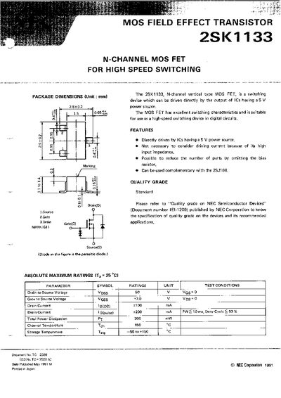
The 2SK1133 is an N‑channel vertical MOSFET designed for high‑speed switching in digital circuits. It can be driven directly from ICs with a 5 V power source and offers low input impedance, reducing the need for external bias resistors.
The document lists key specifications such as voltage and current limits, on‑state resistance, and thermal ratings, and includes recommended surface‑mount soldering conditions for infrared reflow, vapor‑phase, and wave soldering processes.
| Drain‑to‑Source Voltage (VDS) | 50 V |
|---|---|
| Gate‑to‑Source Voltage (VGS) | 7.0 V |
| Continuous Drain Current (ID) | 100 mA |
| Pulse Drain Current (ID(pulse)) | 200 mA |
| Total Power Dissipation (PD) | 200 mW |
| Channel Temperature (Tj) | 150 °C |
| Storage Temperature (Tstg) | -55 °C to +150 °C |
| On‑State Resistance (RDS(on)) – typical | 16 mΩ |
The maximum drain‑to‑source voltage is 50 V.
The device can handle up to 7.0 V gate‑to‑source voltage.
Recommended peak temperatures are 230 °C for infrared reflow, 215 °C for vapor‑phase, and up to 260 °C for wave soldering.