
This document describes the features and dimensions of the SSTA56 / MMSTA56 PNP general purpose transistor. It has a maximum collector-base voltage of -80V and an emitter-base voltage of -4V. The transistor has the same pin dimensions and complements the SSTA06 / MMSTA06. The document also provides packaging and marking specifications, as well as absolute maximum ratings and electrical characteristics.
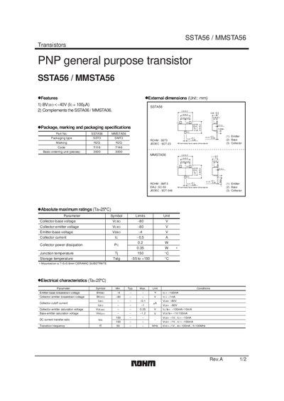
The document describes the SSTA56 and MMSTA56 PNP general‑purpose transistors, highlighting their key features, package options, and typical applications. It includes external dimensions, marking details, and notes on compatibility with related parts.
Detailed electrical specifications are presented, covering absolute maximum ratings, characteristic curves, and typical performance parameters. An appendix contains legal notices, export control information, and usage guidelines for integrating the devices into various electronic equipment.
| Collector‑emitter breakdown voltage (VCEO) | -80 V |
|---|---|
| Collector current (IC) | 0.5 A |
| Power dissipation (Pc) | 0.2 W |
| Junction temperature (Tj) | 150 °C |
| Storage temperature (Tstg) | -55 to +150 °C |
| Package type | SOT‑23 (JEDEC) / SC‑69 (EIAJ) |
| Mounting substrate dimensions | 7 × 5 × 0.6 mm ceramic |
The maximum collector‑emitter voltage is -80 V.
They are available in JEDEC SOT‑23 and EIAJ SC‑69 packages.
The transistors can handle up to 0.5 A of collector current.