
This document describes the features and characteristics of Alliance Semiconductor's AS7C3364PFD32B and AS7C3364PFD36B, including their organization, clock speeds, access time, operation modes, and expandability.
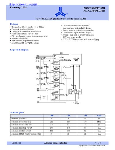
The AS7C3364PFD32B and AS7C3364PFD36B are high‑performance 2‑Mb CMOS synchronous SRAMs organized as 65,536 words × 32 or 36 bits. They feature a two‑stage register‑to‑register pipeline, fast clock speeds up to 200 MHz, and support both interleaved and linear burst modes.
The devices operate from a 3.3 V core supply with optional 2.5 V I/O, are offered in a 100‑pin TQFP package, and include features such as double‑cycle deselect, snooze low‑power mode, and multiple chip‑enable inputs for easy expansion.
| Organization | 65,536 words × 32 or 36 bits |
|---|---|
| Core supply voltage | 3.3 V |
| Maximum clock frequency | 200 MHz (166 MHz, 133 MHz options) |
| Clock‑to‑data access time | 3.0 ns / 3.5 ns / 4.0 ns |
| OE access time | 3.0 ns / 3.5 ns / 4.0 ns |
| Maximum operating current | 375 mA (200 MHz), 350 mA (166 MHz), 325 mA (133 MHz) |
| Package type | 100‑pin TQFP (14 × 20 mm) |
| Input capacitance | 5 pF (typical) |
The core supply voltage is 3.3 V.
They are offered in a 100‑pin TQFP package (14 × 20 mm).
The devices support up to 200 MHz, with lower options of 166 MHz and 133 MHz.
They have three chip‑enable (CE) inputs for easy memory expansion.