
AS7C3364NTF32B and AS7C3364NTF36B are 3.3V 64K × 32/36 flow-through synchronous SRAMs with NTD™ architecture for efficient bus operation. They feature fast clock to data access, fast OE access time, fully synchronous operation, flow-through mode, asynchronous output enable control, 100-pin TQFP package, byte write enables, operation hold clock enable, multiple chip enables for easy expansion, 3.3V core power supply, 2.5V or 3.3V I/O operation with separate VDDQ, self-timed write cycles, interleaved or linear burst modes, and snooze mode for standby operation.
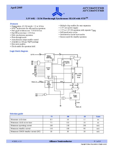
The AS7C3364NTF32B/36B family is a high‑performance 2 Mbit synchronous SRAM organized as 65,536 words × 32 or 36 bits. It uses Alliance’s No Turnaround Delay (NTD) architecture to improve bandwidth and supports both flow‑through and pipelined burst modes. Features include fast clock‑to‑data access, byte‑write enables, multiple chip‑enable expansion, and a low‑power snooze mode.
The device operates from a 3.3 V core supply (±5 %) with separate I/O supplies of 2.5 V or 3.3 V, and is offered in a 100‑pin TQFP package. Electrical specifications cover access times, standby current, absolute maximum ratings, and recommended operating conditions for both 3.3 V and 2.5 V I/O operation.
| Organization | 65,536 words × 32 or 36 bits |
|---|---|
| Fast clock‑to‑data access time | 7.5/8.0/10.0 ns |
| Fast OE access time | 3.5/4.0 ns |
| Core supply voltage | 3.3 V ±5 % |
| Package | 100‑pin TQFP |
| Maximum standby current | 110 mA (3.3 V), 100 mA (2.5 V), 90 mA (other) |
| Power dissipation | 1.8 W |
| Storage temperature range | -65 °C to +150 °C |
The device provides a fast clock‑to‑data access time of 7.5 ns, 8.0 ns, or 10.0 ns depending on the configuration.
Maximum standby current is 110 mA at 3.3 V, 100 mA at 2.5 V, and 90 mA for other variants.
The SRAM is available in a 100‑pin TQFP package.
The core supply voltage is 3.3 V with a tolerance of ±5 %.