
ASM5I961P is a 2.5V or 3.3V compatible, 1:18 PLL based zero delay buffer. With output frequencies of up to 200MHz, output skews of 150pS the device meets the needs of the most demanding clock tree applications.
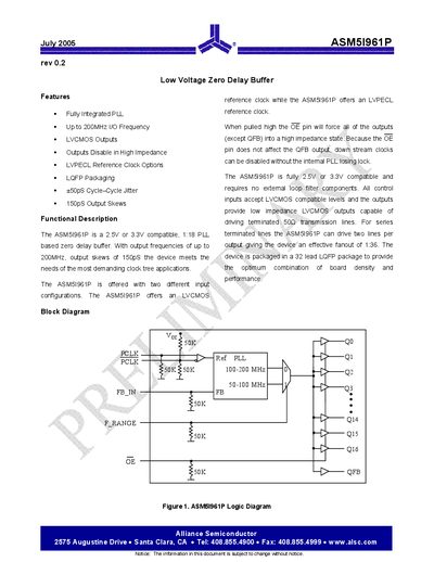
The ASM51961P is a 2.5 V or 3.3 V compatible low‑voltage zero‑delay buffer that incorporates a fully integrated PLL. It provides LVCMOS outputs, optional LVPECL reference clock, and can drive terminated 50 Ω transmission lines without external loop‑filter components.
Key features include up to 200 MHz I/O frequency, 150 ps output skew, +50 ps cycle‑to‑cycle jitter, and an effective fanout of 1:36. The device is supplied in a 32‑lead LQFP package and offers both parallel and series termination options for flexible clock‑tree designs.
| Supply Voltage Range | -0.3 V to 3.6 V |
|---|---|
| Input Frequency Range | 100 MHz – 200 MHz |
| Maximum Output Frequency | 200 MHz |
| Output Skew | 150 ps |
| Output Impedance | 14 Ω – 20 Ω |
| Maximum PLL Lock Time | 40 ms |
| Effective Fanout | 1:36 |
The device supports up to 200 MHz I/O frequency.
It can operate from –0.3 V up to 3.6 V.
It provides an effective fanout of 1:36, allowing two lines per output.
The output impedance is specified between 14 Ω and 20 Ω.