
This document describes the features of AT45DB021D, AT45DB021D is a 2.7V, serial-interface Flash memory, ideally suited for a wide variety of digital voice-, image-, program code- and data-storage applications.
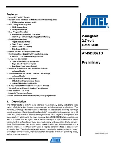
The AT45DB021D is a 2.7 V to 3.6 V serial‑interface Flash memory offering up to 66 MHz RapidS® clock rates. It provides 1,024 pages of 256 bytes or 264 bytes each, a single 256‑byte SRAM buffer, and flexible erase options (page, block, sector, chip). Low‑power operation includes 7 mA active read current, 25 pA standby current and 5 pA deep‑power‑down current.
The device is accessed via a three‑wire SPI‑compatible interface (CS, SI, SO, SCK) with optional write‑protect and reset pins. Detailed command sets cover continuous array reads, page reads, buffer reads, and program/erase operations, all self‑timed and supporting up to 100 k program/erase cycles per page with 20‑year data retention.
| Supply Voltage | 2.7 V to 3.6 V |
|---|---|
| Maximum Clock Frequency | 66 MHz |
| Page Size | 256 bytes or 264 bytes |
| Number of Pages | 1,024 |
| Erase Options | Page (256 B), Block (2 KB), Sector (32 KB), Chip (2 Mbits) |
| Active Read Current | 7 mA typical |
| Standby Current | 25 pA typical |
| Deep Power‑Down Current | 5 pA typical |
| Program/Erase Cycle Endurance | 100,000 cycles per page minimum |
| Data Retention | 20 years |
It operates from a single supply of 2.7 V to 3.6 V for both programming and reading.
The RapidS serial interface supports up to 66 MHz clock frequency.
The device contains 1,024 pages of either 256 bytes or 264 bytes each.
It offers page erase (256 B), block erase (2 KB), sector erase (32 KB) and chip erase (2 Mbits).