
7663B-8051 is an MCU with 80C52 compatibility and 8051 instruction compatibility, featuring six 8-bit I/O ports, three 16-bit timers/counters, 256 bytes of scratch pad RAM, 11 interrupt sources with 4 priority levels. The chip uses standard VCC power supply, integrated power monitor (POR/PFD) to supervise internal power supply, and contains serial loader for in-system programming.
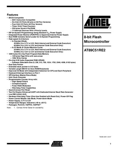
This manual describes the AT89C51RE2 8‑bit Flash microcontroller, its high‑speed architecture, memory organization, and peripheral set. It includes a feature list, block diagram, pin configurations, and detailed SFR mapping for developers.
The document also covers electrical characteristics, package options, and ordering information, along with Atmel contact details for support and literature requests.
| Flash memory size | 128 Kbytes |
|---|---|
| Expanded RAM (XRAM) size | 8192 bytes |
| Operating voltage | 2.7 V to 5.5 V |
| Temperature range | -40 °C to +85 °C (Industrial) |
| Available packages | PLCC44, VQFP44, VQFP64 |
| Maximum CPU frequency (standard mode) | 40 MHz |
| Maximum CPU frequency (high‑voltage mode) | 60 MHz |
| Interrupt sources | 11 sources with 4 priority levels |
| I/O ports | Six 8‑bit ports (64‑pin or 68‑pin versions) |
The AT89C51RE2 contains 128 Kbytes of on‑chip flash program/data memory.
It operates from 2.7 V up to 5.5 V.
The device provides 11 interrupt sources with four priority levels.
It is available in PLCC44, VQFP44 and VQFP64 packages.