
This document introduces the features and characteristics of AT49F080, including single voltage operation, fast read access time, internal program control and timer, 16K bytes boot block lockout, fast erase cycle time, byte programming, hardware data protection, data polling to detect end of program, low power dissipation and typical 10,000 write cycles.
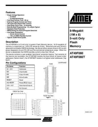
The AT49F080/AT49F080T is a 5‑volt‑only in‑system Flash Memory device offering 8 Mbit (1,024,576 × 8‑bit) storage. It features fast 90 ns read access, 10 µs byte‑programming, 10‑second erase cycles, and a 16 KB boot block with optional lockout for secure code. Typical endurance exceeds 10 000 write cycles while active current is 50 mA and standby current is 100 µA.
The device supports multiple operating modes, including read, program, erase, and product identification. End‑of‑cycle detection can be performed via DATA polling, a toggle‑bit on I/O6, or the open‑drain RDY/BUSY pin. Pin configurations are provided for SOIC, TSOP, and CBGA packages, and ordering information lists commercial and industrial variants with part numbers such as AT49F080‑90CC and AT49F080T‑12RC.
| Operating voltage | 5 V (single voltage operation) |
|---|---|
| Read access time | 90 ns |
| Byte‑programming time | 10 µs per byte (typical) |
| Erase cycle time | 10 seconds (typical) |
| Typical write cycles | 10 000 |
| Active current | 50 mA |
| Boot block size | 16 KB |
| Operating temperature range | -55 °C to +125 °C (absolute max) |
| Package types | 42‑Ball CBGA (4202), 44‑Lead SOIC (44R), 40‑Lead TSOP (40T) |
The AT49F080 operates on a single 5 V supply.
It typically supports up to 10 000 write cycles.
By enabling the boot block lockout feature, the 16 KB boot block becomes write‑protected.
End of a cycle can be detected using DATA polling, the toggle bit on I/O6, or the RDY/BUSY pin.