
The ATF20V8B is a high performance CMOS (Electrically Erasable) Programmable Logic Device (PLD) that utilizes Atmel's proven electrically erasable Flash memory technology. Speeds down to 7.5 ns and power dissipation as low as 10 mA are offered. All speed ranges are specified over the full 5V ± 10% range for industrial temperature ranges, and 5V ± 5% range for commercial temperature ranges.
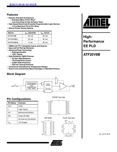
The ATF20V8B is a high‑performance CMOS electrically erasable programmable logic device (PLD) offering 7.5 ns maximum pin‑to‑pin delay, low power consumption, and a superset of generic architectures for direct replacement of many 24‑pin PALs. It includes internal input and I/O pull‑up resistors, multiple power‑saving options, and a 64‑bit user signature area.
The datasheet lists electrical characteristics, timing parameters, and packaging options such as 28‑lead PLCC and 24‑lead PDIP. It also describes programming/erasing procedures, power‑up reset behavior, and compiler mode selection for registered, combinatorial, and simple configurations.
| Maximum Pin‑to‑Pin Delay | 7.5 ns |
|---|---|
| Power Supply Voltage (Commercial) | 5 V ±5 % |
| Power Supply Voltage (Industrial) | 5 V ±10 % |
| Stand‑by Current (ATF20V8B) | 50 mA |
| Active Current (ATF20V8B) | 55 mA |
| Input Low Voltage | -0.5 V |
| Input High Voltage | 2.0 V |
| Power‑Up Reset Time | 600 ns typical, 1 000 ns max |
| Package (PLCC) | 28‑lead PLCC |
| Package (PDIP) | 24‑lead PDIP |
The device has a maximum pin‑to‑pin delay of 7.5 ns.
Commercial devices operate at 5 V ±5 % and industrial devices at 5 V ±10 %.
The ATF20V8B contains eight configurable macrocells.
The power‑up reset voltage is specified as 3.8 V to 4.5 V.