
This document introduces the features and characteristics of LM3671 step-down DC-DC converter. LM3671 step-down DC-DC converter is designed for power supply low voltage circuits from a single Li-Ion cell battery and input voltage rails from 2.7V to 5.5V. The chip provides up to 600mA load current, over the entire input voltage range. There are several different fixed voltage output options available as well as an adjustable output voltage version. The device offers superior features and performance for mobile phones and similar portable systems. Automatic in- telligent switching between PWM low-noise and PFM low- current mode offers improved system control. During PWM mode, the device operates at a fixed-frequency of 2 MHz (typ). Hysteretic PFM mode extends the battery life by re- ducing the quiescent current to 16 µA (typ) during light load and standby operation. Internal synchronous rectification provides high efficiency during PWM mode operation. In shutdown mode, the device turns off and reduces battery consumption to 0.01 µA (typ). The LM3671 is available in SOT23-5 and a tiny 5-bump micro SMD packages in leaded (PB) and lead-free (NO PB) versions. A high switching frequency of 2 MHz (typ) allows use of tiny surface-mount components. Only three external surface-mount components, an inductor and two ceramic capacitors, are required.
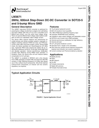
The LM3671 step‑down DC‑DC converter is designed for powering low‑voltage circuits from a single Li‑ion cell or a 2.7 V‑5.5 V input rail. It delivers up to 600 mA load current and switches at a typical 2 MHz frequency, offering both PWM and PFM modes for efficiency and low‑quiescent operation.
The device is offered in two compact packages (SOT23‑5 and 5‑bump micro SMD) and requires only three external components – an inductor and two ceramic capacitors – making it suitable for mobile phones, PDAs, MP3 players, WLAN modules, and other portable electronics.
| Input Voltage Range | 2.7 V to 5.5 V |
|---|---|
| Maximum Load Current | 600 mA |
| Typical Quiescent Current | 16 pA |
| Typical Shutdown Current | 0.01 pA |
| Switching Frequency (PWM mode) | 2 MHz (typ) |
| External Components Required | 1 inductor + 2 ceramic capacitors |
| Package Options | SOT23‑5, 5‑bump micro SMD |
The LM3671 has a typical quiescent current of 16 pA.
It operates with an input voltage from 2.7 V to 5.5 V.
Only three external components are required: one inductor and two ceramic capacitors.
The device is offered in SOT23‑5 and 5‑bump micro SMD packages.