
The CLC5957 is a monolithic 12-bit, 70 MSPS analog-to-digital converter. It is optimized for use in IF-sampled digital receivers and other applications that require high resolution, high sampling rate, wide dynamic range, low power dissipation, and compact size. The CLC5957 features include differential analog inputs, low jitter differential universal clock inputs, a low distortion track-and-hold with 0-300MHz input bandwidth, a bandgap voltage reference, data valid clock output, TTL compatible CMOS (3.3V or 2.5V) programmable output logic, and a proprietary 12-bit multi-stage quantizer. It is fabricated on the ABIC-V 0.8 micron BiCMOS process. The CLC5957 has a spurious free dynamic range (SFDR) of 74dBc and a signal to noise ratio (SNR) of 67dB. The wideband track-and-hold allows sampling of IF signals up to 250MHz. It produces a two-tone, dithered, SFDR of 83dBFS at a 75MHz input frequency. The differential analog input provides excellent common mode rejection, while the differential universal clock inputs minimize jitter. The 48-pin TSSOP package is ideal for space-constrained applications. The CLC5957 operates from a single +5V power supply and is guaranteed to operate over the industrial temperature range of -40˚C to +85˚C. National Semiconductor tests each part to verify compliance with the guaranteed specifications.
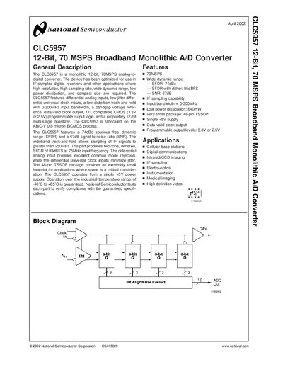
The CLC5957 is a monolithic 12‑bit, 70 MSPS analog‑to‑digital converter optimized for IF‑sampled digital receivers and other high‑speed applications. It features differential analog inputs, a low‑jitter universal clock, a 0‑300 MHz track‑and‑hold bandwidth, and programmable 3.3 V or 2.5 V CMOS output logic. The device operates from a single +5 V supply and is qualified over an industrial temperature range of –40 °C to +85 °C.
The handbook provides pin configurations, absolute maximum ratings, electrical characteristics, typical performance graphs, ordering information, and details of the CLC5957 evaluation board. It also includes mechanical dimensions for the 48‑lead TSSOP package and a life‑support policy notice.
| Input Bandwidth | 0‑300 MHz |
|---|---|
| Signal‑to‑Noise Ratio (SNR) | 67 dB |
| Package | 48‑pin TSSOP |
| Supply Voltage | +5 V |
| Operating Temperature Range | -40 °C to +85 °C |
It operates from a single +5 V supply.
The input bandwidth spans from 0 MHz to 300 MHz.