
This document introduces the characteristics of ADC14L040 14-Bit, 40 MSPS, 235 mW A/D Converter, including single +3.3V supply, 14-bit resolution, 40 MSPS sampling rate, 150 MHz bandwidth, etc.
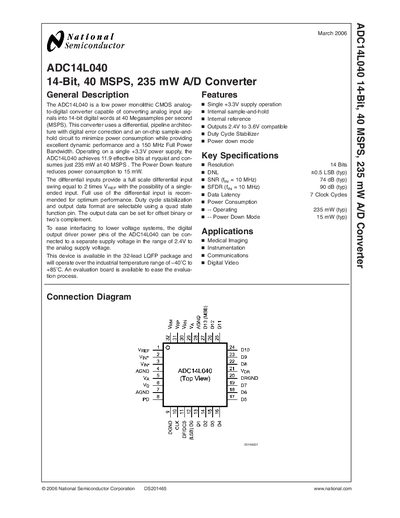
The ADC14L040 is a low‑power monolithic CMOS analog‑digital converter capable of converting analog inputs to 14‑bit digital words at 40 MSPS. It operates from a single +3.3 V supply, offers selectable output formats (offset binary or two’s complement) via the DF/DCS pin, and includes a power‑down mode that reduces consumption to 15 mW.
The document provides detailed pin descriptions, electrical characteristics, absolute maximum ratings, and application notes. It includes ordering information, a block diagram, and physical dimensions for the 32‑lead LQFP package, as well as guidelines for layout, grounding, and reference pin usage.
| Resolution | 14 Bits |
|---|---|
| Maximum Sample Rate | 40 MSPS |
| Typical Power Consumption | 235 mW |
| Power‑Down Consumption | 15 mW (typ) |
| Data Latency | 7 Clock Cycles |
| Maximum Clock Frequency | 40 MHz (min) |
The ADC14L040 consumes about 235 mW at 40 MSPS under typical conditions.
The DF/DCS pin selects the output format: offset binary with duty‑cycle stabilization, or two’s complement without it.
In power‑down mode the device draws approximately 15 mW.
The device supports a minimum maximum clock frequency of 40 MHz.