
This document describes a CMOS device with enhanced performance, which contains two independent positive-edge-triggered D-type flip-flops. It features low power consumption and high-speed switching noise suppression.
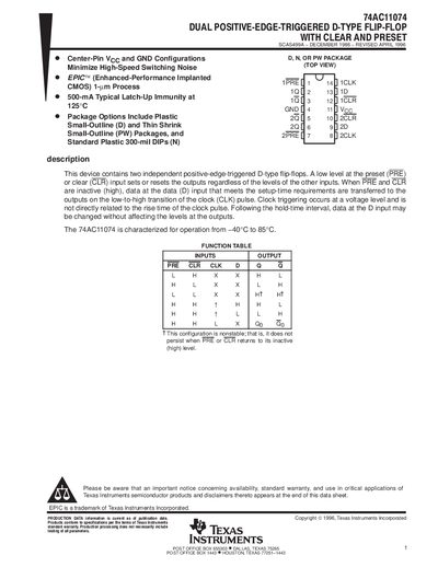
The 74AC11074 is a dual positive‑edge‑triggered D‑type flip‑flop that includes independent clear (CLR) and preset (PRE) inputs. When PRE and CLR are inactive, data on the D input is transferred to the Q outputs on the rising edge of the clock (CLK) provided setup‑time requirements are met.
The device is offered in multiple package options (SOIC, PDIP, TSSOP, etc.) and is characterized for operation from –40 °C to 85 °C with a supply voltage range of 0.5 V to 7 V. Electrical ratings, timing parameters, and maximum power dissipation values are detailed, and an important notice regarding availability and warranty appears at the end of the document.
| Supply voltage range | 0.5 V to 7 V |
|---|---|
| Operating temperature range | -40 °C to 85 °C |
| Maximum power dissipation (D package) | 1.25 W |
| Continuous output current (VQ = 0 V) | 50 mA |
The device operates with a supply voltage from 0.5 V up to 7 V.
It is specified for operation from –40 °C to 85 °C.
The device can operate at clock frequencies up to 125 MHz, depending on the supply voltage.