
CD54ACT112, CD74ACT112 are two dual J-K negative-edge-triggered flip-flops with clear and preset functions produced by TI. This datasheet provides detailed information on the features and characteristics of the two products, pin functions, package types, supply voltages, working temperature ranges, application circuits, etc.
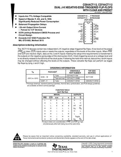
The CD54ACT112 and CD74ACT112 devices contain two independent J‑K negative‑edge‑triggered flip‑flops. A low level on the PRE (preset) or CLR (clear) inputs forces the outputs regardless of other inputs, while normal data transfer occurs on the falling edge of the clock when PRE and CLR are high. The devices support toggle operation by tying J and K high and offer TTL‑compatible inputs.
The datasheet provides electrical characteristics, absolute‑maximum ratings, recommended operating conditions, timing requirements, and switching characteristics. Packaging options include CDIP, SOIC, and tape‑and‑reel formats, with detailed mechanical drawings and thermal data. An important notice outlines warranty, usage restrictions, and regulatory information.
| Supply voltage range (VCC) | 4.5 V – 5.5 V |
|---|---|
| Output drive current (I_OH / I_OL) | ±24 mA |
| Fanout | 15 F devices |
| Maximum clock frequency (fmax) | 100 MHz – 114 MHz |
| High‑level input voltage (VIH) | 2 V |
| Low‑level input voltage (VIL) | 0.8 V |
The devices operate with a supply voltage between 4.5 V and 5.5 V.
Each output can source or sink up to ±24 mA.
They are offered in CDIP (tube) and SOIC (surface‑mount) packages, with tape‑and‑reel options.
The devices support clock frequencies from 100 MHz up to 114 MHz.