
SN74LVC112A is a dual negative-edge-triggered J-K flip-flop with clear and preset functions. It operates from 1.65V to 3.6V and accepts input voltages up to 5.5V. It has a fast propagation delay and stable output levels. Can be used as a flip-flop or toggle flip-flop.
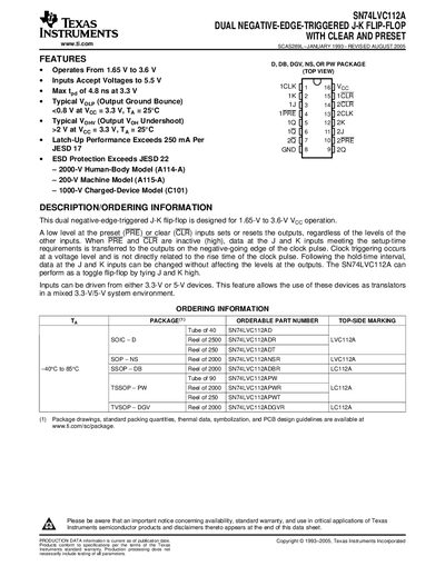
The SN74LVC112A is a dual negative‑edge‑triggered J‑K flip‑flop that includes clear (CLR) and preset (PRE) inputs. It operates from 1.65 V to 3.6 V and can accept input voltages up to 5.5 V, making it suitable for mixed‑voltage systems.
The document provides detailed electrical characteristics, absolute maximum ratings, recommended operating conditions, timing requirements, and packaging information for various SOIC, SSOP, TSSOP, and TVSOP options. It also includes ESD protection specifications and mechanical drawings.
| Recommended supply voltage range | 1.65 V to 3.6 V |
|---|---|
| Maximum input voltage | 5.5 V |
| Continuous output current | +50 mA |
| Continuous current through VCC or GND | +100 mA |
| Storage temperature range | -65 °C to 150 °C |
| Operating free‑air temperature range | -40 °C to 85 °C |
| ESD protection (Human‑Body Model) | 2000 V |
The device is recommended to operate from 1.65 V to 3.6 V.
It meets JESD‑22 standards with 2000 V Human‑Body Model, 200 V Machine Model, and 1000 V Charged‑Device Model protection.
The part can be stored from –65 °C up to 150 °C.
It can source or sink up to 50 mA continuously on the output and up to 100 mA through VCC or GND.