
The SN74F112 is a dual negative-edge-triggered J-K flip-flop with clear and preset functions. It contains two independent J-K flip-flops. A low level at the preset or clear inputs sets or resets the outputs regardless of the levels of the other inputs. Data at the J and K inputs meeting the setup time requirements is transferred to the outputs on the negative-going edge of the clock pulse. Clock triggering occurs at a voltage level and is not directly related to the rise time of the clock pulse. Following the hold-time interval, data at the J and K inputs may be changed without affecting the levels at the outputs. The SN74F112 can perform as a toggle flip-flop by tying J and K high. The device is characterized for operation from 0°C to 70°C.
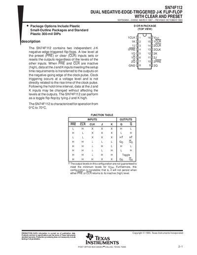
The SN74F112 contains two independent J‑K flip‑flops that trigger on the negative‑going edge of the clock. A low level on the PRE or CLR inputs forces the outputs to a defined state regardless of other inputs, and the device operates from 0 °C to 70 °C.
The part is offered in several SOIC and PDIP packages, supports a supply voltage from –0.5 V to 7 V, and provides defined input and output current limits. Detailed electrical characteristics, timing parameters, and packaging dimensions are listed in the datasheet.
| Supply voltage range (VCC) | –0.5 V to 7 V |
|---|---|
| Input voltage range (VI) | –1.2 V to 7 V |
| Input current range | –30 mA to 5 mA |
| Low‑level output current (IOL) | 20 mA |
| Operating temperature range | 0 °C to 70 °C |
| Package types | SOIC (16‑pin) and PDIP (16‑pin) |
The device operates with a supply voltage from –0.5 V to 7 V.
It is specified for operation from 0 °C up to 70 °C.
The part is offered in SOIC and PDIP packages, both with 16 pins.
Input voltages may range from –1.2 V to 7 V.