
The MAX9205/MAX9207 serializers transform 10-bit-wide parallel LVCMOS/LVTTL data into a serial high-speed bus low-voltage differential signaling (LVDS) data stream. The serializers typically pair with deserializers like the MAX9206/MAX9208, which receive the serial output and transform it back to 10-bit-wide parallel data. The MAX9205/MAX9207 transmit serial data at speeds up to 400Mbps and 660Mbps, respectively, over PCB traces or twisted-pair cables. Since the clock is recovered from the serial data stream, clock-to-data and data-to-data skew that would be present with a parallel bus are eliminated. The serializers require no external components and few control signals. The input data strobe edge is selected by TCLK_R/F. PWRDN is used to save power when the devices are not in use. Upon power-up, a synchronization mode is activated, which is controlled by two SYNC inputs, SYNC1 and SYNC2. The MAX9205 can lock to a 16MHz to 40MHz system clock, while the MAX9207 can lock to a 40MHz to 66MHz system clock. The serializer output is held in high impedance until the device is fully locked to the local system clock, or when the device is in power-down mode. Both the devices operate from a single +3.3V supply, are specified for operation from -40°C to +85°C, and are available in 28-pin SSOP packages.
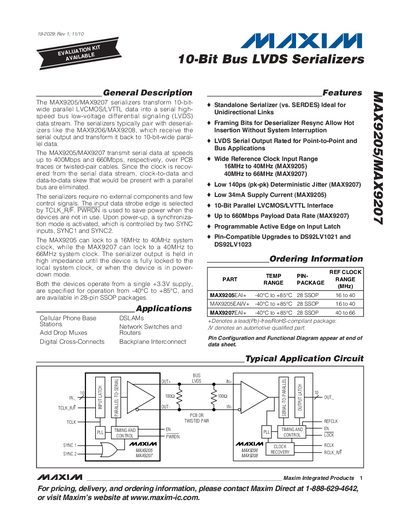
The MAX9205 and MAX9207 are 10‑bit LVDS serializers that convert parallel LVCMOS/LVTTL data into a high‑speed serial LVDS stream. They operate from a single +3.3 V supply and support reference clocks from 16 MHz to 66 MHz, delivering up to 400 Mbps (MAX9205) or 660 Mbps (MAX9207) over PCB traces or twisted‑pair cables.
The devices include built‑in power‑down control, synchronization pins, and are offered in a 28‑pin SSOP package. Detailed electrical characteristics, pin functions, and application guidelines are provided for point‑to‑point and multipoint bus implementations.
| Maximum Serial Data Rate (MAX9207) | 660 Mbps |
|---|---|
| Supply Voltage | +3.3 V |
| Package | 28‑pin SSOP |
| Operating Temperature Range | -40 °C to +85 °C |
| Reference Clock Input (MAX9205) | 16 MHz to 40 MHz |
| Reference Clock Input (MAX9207) | 40 MHz to 66 MHz |
Power‑down is entered by driving the PWRDN pin low, which stops the PLL and places the LVDS outputs in high‑impedance.
Both devices operate from a single +3.3 V supply.
They are offered in a 28‑pin SSOP package.