
The MAX9209/MAX9213 is a serializer produced by TI. It supports 21-bit LVTTL/LVCMOS parallel input data and outputs three LVDS signals. A fourth LVDS signal provides a deserialization clock. The product has a programmable DC balance function, which can achieve isolation between the serializer and the deserializer using AC coupling. The DC balance circuit on each channel encodes the data, limiting the imbalance of transmitted 1s and 0s to a defined range. The companion MAX9210/MAX9214 deserializers decode the data. When DC balance is not programmed, the serializers are compatible with non-DC-balanced, 21-bit serializers such as the DS90CR215 and DS90CR217. Two frequency ranges and two DC-balance default conditions are available for maximum replacement flexibility and compatibility with existing non-DC-balanced serializers. MAX9209/MAX9213 is available in TSSOP and space-saving TQFN packages.
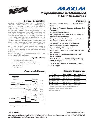
The MAX9209 and MAX9213 serialize 21 bits of LVTTL/LVCMOS parallel data to three LVDS outputs with an optional fourth LVDS clock output. They feature programmable DC‑balance, allowing AC‑coupled isolation between serializer and deserializer, and are pin‑compatible with DS90CR215/DS90CR217 in non‑DC‑balanced mode.
Available in 48‑lead TSSOP and space‑saving 48‑lead TQFN packages, the devices operate from –40 °C to +85 °C, support up to 66 MHz parallel clock rates, and provide integrated LVDS termination resistors (110 Ω DC‑balanced, 410 Ω non‑DC‑balanced). Detailed electrical characteristics, pin descriptions, layout recommendations, and ESD protection specifications are included.
| Operating Temperature Range | -40 °C to +85 °C |
|---|---|
| Supply Voltage (VCC) | +3.0 V to +3.6 V |
| Maximum Data Rate (DC‑balanced) | 594 Mbps |
| Package Types | 48‑Lead TSSOP, 48‑Lead TQFN |
The MAX9213 can achieve up to 594 Mbps in DC‑balanced mode (66 MHz × 9 bits).
DC‑balance is controlled by the DCB/NC pin; setting it high enables DC‑balanced operation, low selects non‑DC‑balanced mode.
In DC‑balanced mode the termination is 110 Ω; in non‑DC‑balanced mode it is 410 Ω (typical).
They are offered in a 48‑lead low‑profile TSSOP and a space‑saving 48‑lead TQFN package.