
The AOD425 is a P-channel enhancement mode field effect transistor from Alpha & Omega Semiconductor, Ltd. It features low RDS(ON) (≤17mΩ) and ultra-low gate charge (≤11 nC). This device is suitable for use as a load switch or in PWM applications.
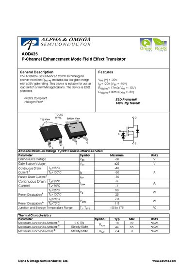
The AOD425 is a P‑Channel Enhancement Mode Field Effect Transistor using advanced trench technology. It is designed for load‑switch and PWM applications with a drain‑source voltage rating of –30 V and a gate‑source rating of +25 V.
The datasheet lists absolute maximum ratings, thermal characteristics, and detailed electrical parameters such as drain current, on‑resistance, gate charge, and capacitances. Typical performance curves and test circuit waveforms illustrate on‑region behavior, switching speed, and diode recovery characteristics.
| Drain‑Source Voltage (VDS) | -30 V |
|---|---|
| Gate‑Source Voltage (VGS) | +25 V |
| Continuous Drain Current (ID) at 25 °C | -20 A |
| Pulsed Drain Current (ID,pulse) | -70 A |
| Power Dissipation at 70 °C | 1.5 W |
| Junction Temperature Range | -55 °C to 175 °C |
| Gate Threshold Voltage (Vth) | -1.5 V to -3.5 V |
The AOD425 is rated for a maximum drain‑source voltage of –30 V.
The device can handle a gate‑source voltage up to +25 V.