
The MAX2837 is a direct-conversion zero-IF RF transceiver designed specifically for 2.3GHz to 2.7GHz wireless broadband systems. It integrates all circuitry required to implement the RF transceiver function, including RF-to-baseband receive path, baseband-to-RF transmit path, VCO, frequency synthesizer, crystal oscillator, and baseband/control interface. The device also includes circuits for on-chip DC offset cancellation, I/Q error, and carrier-leakage detection. Only a few external components are needed to form a complete wireless broadband RF radio solution, including an RF bandpass filter (BPF), crystal, RF switch, PA, and passive components. The MAX2837 eliminates the need for an external SAW filter by implementing on-chip monolithic filters for both the receiver and transmitter. The baseband filters and Rx/Tx signal paths are optimized to meet stringent noise figure and linearity specifications. The device supports up to 2048 FFT OFDM and implements programmable channel filters for RF channel bandwidths ranging from 1.75MHz to 28MHz. The transceiver has a fast 2µs Tx-Rx switching time, including frequency transient settling. It is available in a small 48-pin thin QFN package measuring only 6mm x 6mm x 0.8mm.
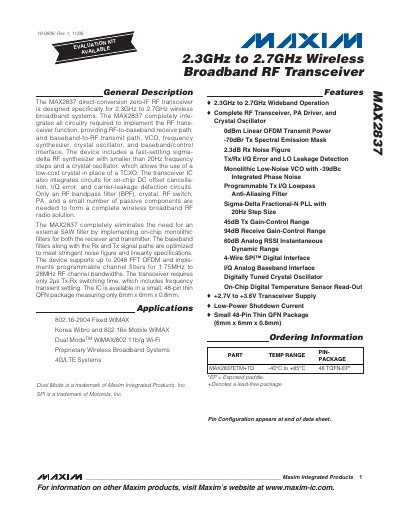
The MAX2837 direct‑conversion zero‑IF RF transceiver is designed for 2.3 GHz to 2.7 GHz wireless broadband systems. It integrates the complete RF‑to‑baseband receive path, baseband‑to‑RF transmit path, VCO, frequency synthesizer, crystal oscillator and control interface, and includes on‑chip DC offset cancellation, I/Q error correction and carrier‑leakage detection.
The device is supplied in a 48‑pin thin QFN package (6 mm × 6 mm × 0.8 mm) and operates from 2.7 V to 3.6 V. Key performance figures include a 2 µs Tx‑Rx switching time, 2.3 dB Rx noise figure, 0 dBm maximum output power and a supply‑current range of 0 µA (shutdown) to 170 mA (Tx mode).
| Operating Frequency Range | 2.3 GHz – 2.7 GHz |
|---|---|
| Package | 48‑pin thin QFN, 6 mm × 6 mm × 0.8 mm |
| Supply Voltage | 2.7 V – 3.6 V |
| Tx‑Rx Switching Time | 2 µs |
| Rx Noise Figure | 2.3 dB |
| Operating Temperature Range | -40 °C – +85 °C |
It operates from 2.3 GHz to 2.7 GHz.
A 48‑pin thin QFN package measuring 6 mm × 6 mm × 0.8 mm.
The device operates from 2.7 V to 3.6 V.
The transceiver switches in 2 µs.