
The MAX2839AS is a direct conversion, zero-IF, RF transceiver specifically designed for 2.3GHz to 2.7GHz 802.16e MIMO mobile WiMAX™ systems. The device incorporates one transmitter and two receivers, with > 40dB isolation between each receiver. The MAX2839AS completely integrates all circuitry required to implement the RF transceiver function, providing RF to baseband receive path, and baseband to RF transmit path, VCO, frequency synthesizer, crystal oscillator, and base-band/control interface. The device includes a fast-set- tling sigma-delta RF synthesizer with smaller than 40Hz frequency steps and a crystal oscillator that allows the use of a low-cost crystal in place of a TCXO. The trans- ceiver IC also integrates circuits for on-chip DC-offset cancellation, I/Q error, and carrier leakage detection circuits. An internal transmit to receive loopback mode allows for receiver I/Q imbalance calibration. The local oscillator I/Q quadrature phase error can be digitally corrected in approximately 0.125° steps. Only an RF bandpass filter (BPF), crystal, RF switch, PA, and a small number of passive components are needed to form a complete wireless broadband RF radio solution. The MAX2839AS completely eliminates the need for an external SAW filter by implementing on-chip program- mable monolithic filters for both the receiver and trans- mitter, for all 2GHz and 802.16e profiles and WiBro. The baseband filters along with the Rx and Tx signal paths are optimize for various profiles to achieve optimal performance.
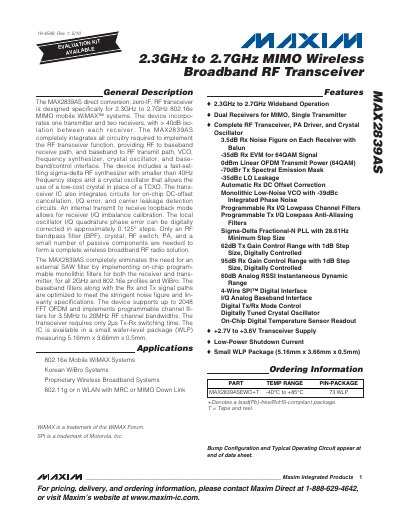
The MAX2839AS is a direct‑conversion, zero‑IF RF transceiver designed for 2.3 GHz to 2.7 GHz 802.16e MIMO mobile WiMAX systems. It integrates one transmitter, two receivers, a VCO, sigma‑delta fractional‑N PLL, crystal oscillator, and on‑chip DC‑offset correction, I/Q error correction, and carrier‑leakage detection. Only a band‑pass filter, crystal, RF switch, PA and a few passive components are needed for a complete wireless broadband solution.
Key features include >40 dB isolation between receivers, 2 µs Tx‑Rx switching time, 62 dB Tx gain control range, 3.5 dB Rx noise figure per receiver, and a small wafer‑level package (5.16 mm × 3.66 mm × 0.5 mm). The device supports up to 2048‑FFT OFDM, programmable channel filters from 3.5 MHz to 20 MHz, and provides a 4‑wire SPI digital interface for configuration.
| Frequency range | 2.3 GHz – 2.7 GHz |
|---|---|
| Package size | 5.16 mm × 3.66 mm × 0.5 mm |
| Supply voltage (VCC) | 2.7 V – 3.6 V |
| Tx‑Rx switching time | 2 µs |
| Tx gain control range | 62 dB |
| Rx noise figure | 3.5 dB per receiver |
| Maximum RF output power | 0 dBm |
The device operates from a supply voltage (VCC) of 2.7 V to 3.6 V.
The transceiver can switch from Tx to Rx (or Rx to Tx) in 2 µs.
It is offered in a wafer‑level package measuring 5.16 mm × 3.66 mm × 0.5 mm.
Each receiver has a noise figure of 3.5 dB.