
The MAX1446 is a 10-bit, 3V analog-to-digital converter (ADC) with a fully differential input, a pipelined 10-stage ADC architecture with digital error correction, and wideband track and hold (T/H) incorporating a fully differential signal path. This ADC is optimized for low-power, high dynamic performance applications in imaging and digital communications. The MAX1446 operates from a single 2.7V to 3.6V supply, consuming only 90mW while delivering a 59.5dB signal-to-noise ratio (SNR) at a 20MHz input frequency. The fully differential input stage has a 400MHz, -3dB bandwidth and may be operated with single-ended inputs. In addition to low operating power, the MAX1446 features a 5µA power-down mode for idle periods. An internal 2.048V precision bandgap reference is used to set the ADC full-scale range. A flexible reference structure allows the user to supply a buffered, direct or externally derived reference for applications requiring increased accuracy or a different input voltage range. Lower and higher speed, pin-compatible versions of the MAX1446 are also available. Refer to the MAX1444 data sheet for a 40Msps version, the MAX1448 data sheet for an 80Msps version, and the MAX1449 data sheet for a 105Msps version. The MAX1446 has parallel, offset binary, three-state outputs that can be operated from 1.7V to 3.3V to allow flexible interfacing. The device is available in a 5mm x 5mm, 32-pin TQFP package and is specified over the extended industrial (-4) temperature range.
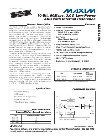
The MAX1446 is a 10‑bit, 3 V analog‑to‑digital converter optimized for low‑power, high‑dynamic‑performance applications such as imaging and digital communications. It operates from a single 2.7 V to 3.6 V supply and consumes only 90 mW in normal mode, with a 5 µA shutdown current.
Key features include a fully differential input with a 400 MHz –3 dB bandwidth, an internal 2.048 V precision bandgap reference, three‑state CMOS‑compatible outputs, and a 32‑pin TQFP package available for industrial (‑40 °C to +85 °C) and automotive (‑40 °C to +105 °C) temperature ranges.
| Resolution | 10 bits |
|---|---|
| Maximum Sampling Rate | 60 Msps (60 MHz clock) |
| Supply Voltage | 2.7 V – 3.6 V |
| Power Consumption (normal) | 90 mW |
| Power‑down Current | 5 µA |
| Input Bandwidth | 400 MHz (‑3 dB) |
| Internal Reference Voltage | 2.048 V |
| Package | 32‑pin TQFP |
| Operating Temperature Range | -40 °C to +85 °C (industrial), -40 °C to +105 °C (automotive) |
The MAX1446 can sample up to 60 Msps, with a maximum clock frequency of 60 MHz.
It consumes only 90 mW while operating at 20 MHz input frequency.
The device has a 5 µA power‑down (shutdown) current.
It is specified for –40 °C to +85 °C (industrial) and –40 °C to +105 °C (automotive) grades.
It includes an internal 2.048 V precision bandgap reference.