
The MAX5893 is a programmable interpolating, modulating, 500Msps, dual digital-to-analog converter (DAC) optimized for high-performance wideband, single-carrier transmit applications. It integrates a selectable 2x/4x/8x interpolating filter, a digital quadrature modulator, and dual 12-bit high-speed DACs on a single integrated circuit. At 30MHz output frequency and 500Msps update rate, the in-band SFDR is 84dBc while consuming 1.1W. The device also delivers 72dB ACLR for single-carrier WCDMA at a 61.44MHz output frequency. The selectable interpolating filters allow lower input data rates while taking advantage of the high DAC update rates. These linear-phase interpolation filters ease reconstruction filter requirements and enhance the passband dynamic performance. Individual offset and gain programmability allow the user to calibrate out local oscillator (LO) feedthrough and sideband suppression errors generated by analog quadrature modulators. The MAX5893 features a fIM/4 digital image-reject modulator. This modulator generates a quadrature-modulated IF signal that can be presented to an analog I/Q modulator to complete the upconversion process. A second digital modulation mode allows the signal to be frequency-translated with image pairs at fIM/2 or fIM/4. The MAX5893 features a standard 1.8V CMOS, 3.3V tolerant data input bus for easy interface. A 3.3V SPI™ port is provided for mode configuration.
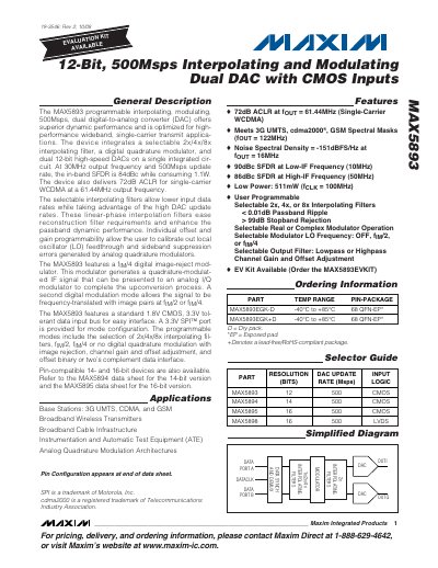
The MAX5893 is a programmable interpolating, modulating, 500 Msps dual digital‑to‑analog converter (DAC) that integrates selectable 2×, 4×, or 8× interpolation filters, a digital quadrature modulator, and two 12‑bit high‑speed DACs on a single IC. It targets high‑performance wideband, single‑carrier transmit applications such as 3G UMTS, CDMA, GSM, and broadband wireless transmitters.
Key specifications include a 12‑bit resolution, up to 500 Msps update rate, in‑band SFDR of 84 dBc at 30 MHz, and 72 dB ACLR for single‑carrier WCDMA at 61.44 MHz. The device operates from 1.8 V CMOS and 3.3 V tolerant inputs, consumes about 511 mW typical power, and offers extensive pin‑level configuration via a 3.3 V SPI interface.
| Resolution | 12 bits |
|---|---|
| Maximum DAC Update Rate | 500 Msps |
| Typical Power Dissipation | 511 mW |
| In‑band SFDR (30 MHz output) | 84 dBc |
| ACLR (61.44 MHz output) | 72 dB |
| Input Logic Voltage Range | 1.8 V CMOS, 3.3 V tolerant |
The MAX5893 can update at up to 500 Msps.
Typical power dissipation is 511 mW.
The device offers selectable 2×, 4×, or 8× interpolation filters.
The data input bus is standard 1.8 V CMOS and 3.3 V tolerant.