
The MAX5889 is a 12-bit, 600Msps digital-to-analog converter (DAC) that meets the demanding performance requirements of signal synthesis applications found in wireless base stations and other communications applications. Operating from 3.3V and 1.8V supplies, the MAX5889 DAC supports update rates of 600Msps using high-speed LVDS inputs while consuming only 292mW of power and offers exceptional dynamic performance such as 79dBc spurious-free dynamic range (SFDR) at fOUT = 30MHz. The MAX5889 utilizes a current-steering architecture that supports a 2mA to 20mA full-scale output current range, and produces -2dBm to -22dBm full-scale output signal levels with a double-terminated 50Ω load. The MAX5889 features an integrated 1.2V bandgap reference and control amplifier to ensure high-accuracy and low-noise performance. A separate reference input (REFIO) allows for the use of an external reference source for optimum flexibility and improved gain accuracy. The MAX5889 digital inputs accept LVDS voltage levels, and the flexible clock input can be driven differentially or single-ended, AC- or DC-coupled. The MAX5889 is available in a 68-pin QFN package with an exposed paddle (EP) and is specified for the extended (-40°C to +85°C) temperature range. Refer to the MAX5891 and MAX5890 data sheets for pin-compatible 16-bit and 14-bit versions of the MAX5889.
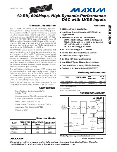
The MAX5889 is a high‑dynamic‑performance digital‑to‑analog converter designed for signal‑synthesis applications such as wireless base stations, DDS and test equipment. It operates from 1.8 V or 3.3 V supplies, consumes only 292 mW at 600 Msps, and provides a spurious‑free dynamic range of 79 dBc at 30 MHz.
Key features include a 12‑bit resolution, LVDS‑compatible digital inputs, an integrated 1.2 V bandgap reference, and a 2 mA‑20 mA full‑scale output current range. The device is offered in a 68‑pin QFN‑EP package and is rated for –40 °C to +85 °C operation.
| Resolution | 12 bits |
|---|---|
| Maximum Update Rate | 600 Msps |
| Power Dissipation | 292 mW |
| Full‑Scale Output Current | 2 mA – 20 mA |
| LVDS Digital Inputs | Yes |
| Integrated Reference | 1.2 V bandgap |
| Operating Temperature Range | -40 °C to +85 °C |
| Spurious‑Free Dynamic Range | 79 dBc at 30 MHz |
| Noise Spectral Density | -157 dBFS/Hz at 36 MHz |
The MAX5889 supports a maximum update rate of 600 Msps.
At 600 Msps the device dissipates about 292 mW of power.
It can deliver a full‑scale output current from 2 mA up to 20 mA.