
TMS320C6713 is the highest-performance floating-point digital signal processor (DSP) from Texas Instruments. It has a 32-bit instruction word width, 32/64-bit data width, and clock frequencies of 300-, 225-, 200-MHz (GDP), and 200-, 167-MHz (PYP). The chip features eight 32-bit instructions/cycle, a rich peripheral set, an optimized C/C++ compiler, and an advanced VLIW DSP core.
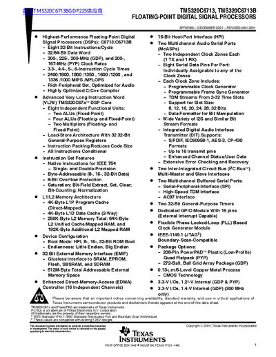
The TMS320C6713 and TMS320C6713B are high‑performance floating‑point digital signal processors featuring an advanced VLIW core with eight independent functional units, 32‑bit general‑purpose registers, and a rich peripheral set optimized for audio applications. The devices support clock rates up to 300 MHz (GDP package) or 200 MHz (PYP package) and deliver up to 2400 MIPS/1800 MFLOPS.
The datasheet includes detailed pin‑assignment tables for the 272‑ball BGA (GDP) and 208‑pin PowerPAD™ QFP (PYP) packages, memory maps, electrical characteristics, and timing specifications for peripherals such as multichannel audio serial ports (McASP), I²C, and EDMA. Revision history and an important notice about product availability and warranty are also provided.
| Clock Rate (GDP package) | 300 MHz, 225 MHz, 200 MHz |
|---|---|
| Clock Rate (PYP package) | 200 MHz, 167 MHz |
| MIPS / MFLOPS | 2400/1800, 1800/1350, 1600/1200, 1336/1000 |
| L1 Program Cache | 4 KB (direct‑mapped) |
| L1 Data Cache | 4 KB (2‑way, external interrupt capable) |
| L2 Memory Total | 256 KB (64 KB unified cache/mapped RAM) |
| General‑Purpose Registers | 32 registers, 32‑bit each |
| Functional Units | Eight (2 Fixed‑Point ALUs, 4 Floating/Fixed‑Point ALUs, 2 Multipliers) |
| Core Supply Voltage (GDP) | 1.20 V |
The device supports 300 MHz, 225 MHz, and 200 MHz clock rates in the GDP package, and 200 MHz and 167 MHz in the PYP package.
It provides a total of 256 KB L2 memory, of which 64 KB is a unified cache/mapped RAM.
The core includes 32 general‑purpose registers, each 32 bits wide.