
This document describes the features and characteristics of the SN54F243 and SN74F243 quadruple bus transceivers. These transceivers are designed for asynchronous communication between data buses and offer flexible timing. They allow data transmission from the A bus to the B bus or from the B bus to the A bus based on the logic levels at the output-enable (OEBA and OEAB) inputs. The output-enable inputs can be used to disable the device, effectively isolating the buses. The dual-enable configuration allows the quadruple bus transceivers to store data by simultaneously enabling OEBA and OEAB. In this configuration, each output reinforces its input. Therefore, when both control inputs are enabled and all other data sources to the two sets of bus lines are in a high-impedance state, both sets of bus lines (eight in total) maintain their states. The 4-bit codes appearing on the two sets of buses will be identical for the ′F243. The SN54F243 is characterized for operation over the full military temperature range of -55°C to 125°C. The SN74F243 is characterized for...
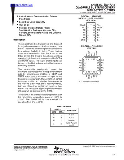
The SN54F243 and SN74F243 are quadruple bus transceivers designed for asynchronous communication between data buses. They provide bidirectional data transfer with independent output‑enable controls, allowing isolation or storage of bus data when both OE inputs are asserted.
The devices operate over a wide temperature range (‑55 °C to 125 °C for SN54F243, 0 °C to 70 °C for SN74F243) and are offered in multiple packages, including plastic small‑outline, ceramic chip carriers, and standard 300‑mil DIP. Key electrical parameters such as supply voltage, input voltage, and output current are specified in the datasheet.
| Package options | Plastic Small‑Outline, Ceramic Chip Carriers, Standard 300‑mil DIPs |
|---|
They are offered in plastic small‑outline packages, ceramic chip carriers, and standard 300‑mil DIP packages.