
This document describes the SD1541-01, a hermetically sealed, gold metallized, silicon NPN power transistor. It is designed for applications requiring high peak power and low duty cycles such as DME. The SD1541-01 is packaged in a hermetic metal/ceramic package with internal input/output matching, resulting in improved broadband performance and low thermal resistance.
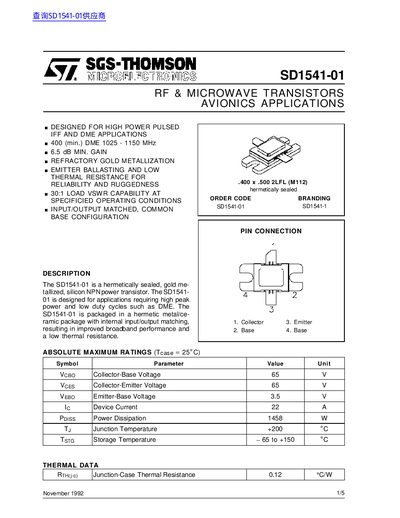
The SD1541‑01 is a hermetically sealed, gold‑metallized silicon NPN power transistor designed for high‑power pulsed IFF and DME applications. It features internal input/output matching, low thermal resistance, and a rugged metal‑ceramic package.
The document provides absolute maximum ratings, electrical specifications, impedance data, pin connections, mechanical dimensions, and typical performance curves for frequencies between 1025 MHz and 1150 MHz.
| Collector‑Base Voltage (VcBO) | 65 V |
|---|---|
| Collector‑Emitter Voltage (VcE) | 65 V |
| Emitter‑Base Voltage (VEB) | 3.5 V |
| Maximum Device Current (Ic) | 22 A |
| Maximum Power Dissipation (Pp) | 1458 W |
| Junction Temperature (Tj) | +200 °C |
| Thermal Resistance (Rth(j‑c)) | 0.12 °C/W |
| Operating Frequency Range | 1025 – 1150 MHz |
The collector‑base voltage rating is 65 V.
It operates from 1025 MHz to 1150 MHz.
The device can dissipate up to 1458 W.