
The M54/74HCT00 is a high speed CMOS QUAD 2-INPUT NAND GATE fabricated in silicon gate C2MOS technology. It has the same highspeed per- formance of LSTTL combined with true CMOS low power consumption. The internal circuit is com- posed of 3 stages including buffer output, which en- ables high noise immunity and stable output. All inputs are equipped with protection circuits against static discharge and transient excess voltage. This integrated circuit has input and output charac- teristics that are fully compatible with 54/74 LSTTL logic families. M54/74HC devices are designed to directly interface HSC2MOS systems with TTL and NMOS components. They are also plug in replace- ments for LSTTL devices giving a reduction of power consumption.
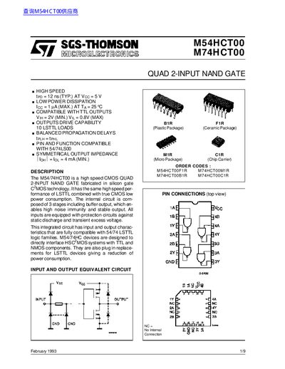
The M54HCT00 and M74HCT00 are high‑speed CMOS quad 2‑input NAND gates compatible with TTL logic families. They feature low power dissipation, balanced propagation delays, and output drive capability suitable for both plastic and ceramic DIP packages.
The document lists absolute maximum ratings, recommended operating conditions, DC and AC electrical specifications, as well as detailed mechanical dimensions for multiple package types (DIP14, DIP14 ceramic, SO14, PLCC20). It also includes truth tables, pin descriptions, and logic diagrams to aid designers in integrating the devices into their circuits.
| Supply voltage (VCC) | 4.5 to 5.5 V |
|---|---|
| Output drive current per pin | 25 mA (max) |
| Power dissipation (Pp) | 500 mW (max) |
| Storage temperature range | -65 to +150 °C |
| Lead temperature (10 s) | 300 °C |
The recommended supply voltage range is 4.5 V to 5.5 V.
Each output pin can source or sink up to 25 mA.
Yes, the gates are fully compatible with TTL output levels.