
The ADF4196 frequency synthesizer can be used to implement local oscillators (LO) in the upconversion and downconversion sections of wireless receivers and transmitters. Its architecture is specifically designed for low phase noise, fast settling, and a 6 GHz PLL frequency synthesizer. It features fast settling, fractional-N PLL architecture, a single PLL that replaces ping-pong synthesizers, frequency hopping across the GSM band in 5 μs with phase settled within 20 μs, 1 degree rms phase error at 4 GHz RF output, digitally programmable output phase, RF input range up to 6 GHz, 3-wire serial interface, on-chip low noise differential amplifier, and a phase noise figure of merit of -216 dBc/Hz.
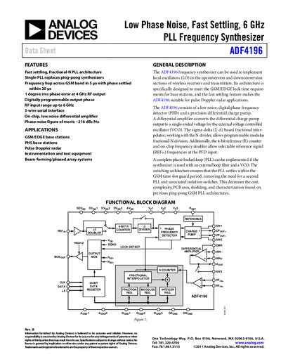
The ADF4196 is a low‑phase‑noise, fast‑settling 6 GHz PLL frequency synthesizer designed for GSM/EDGE base stations, pulse‑Doppler radar, and phased‑array systems. It features a fractional‑N architecture, 3‑wire serial interface, on‑chip differential amplifier, and programmable output phase.
The document includes detailed specifications, absolute maximum ratings, thermal data, pin configuration, SPI‑compatible interfacing guidelines, PCB design recommendations, outline dimensions, and ordering information for the 32‑lead LFCSP package.
| Phase Noise Floor | –216 dBc/Hz |
|---|---|
| Operating Temperature Range | –40 °C to +85 °C |
| AVop Supply Voltage | 2.7 V (min) 3.3 V (typ) |
| Maximum Serial Clock Rate | 33 MHz |
Its phase‑noise floor is –216 dBc/Hz at the VCO output with dither off.
The ADF4196 operates from –40 °C to +85 °C.
The SPI clock can run up to 33 MHz.