
ADM8832 is a charge pump regulator for color TFT panels. It features multiple output voltages, power efficiency optimization, low quiescent current, fast transient response, etc.
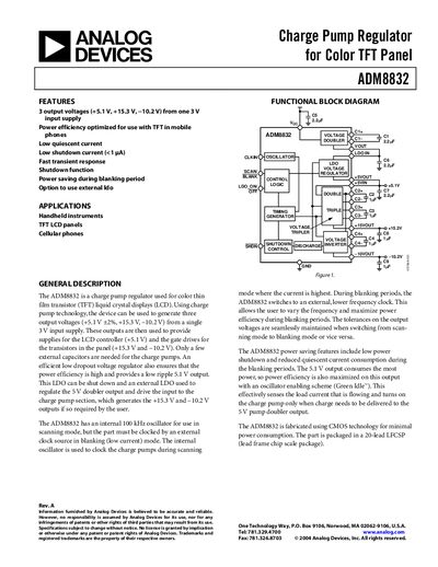
The ADM8832 charge‑pump regulator provides three regulated outputs (+5.1 V, +15.3 V, –10.2 V) from a single 3 V supply, optimized for color TFT LCD panels in handheld devices. It includes an internal LDO for the +5.1 V output, a voltage doubler, tripler and inverter, and supports low‑quiescent and shutdown operation to save power during blanking periods.
The device features an internal 100 kHz oscillator for scanning mode and can be driven by an external clock (minimum 1 kHz) in blanking mode. Pin functions, timing specifications, absolute maximum ratings, and typical performance curves are detailed in the document, along with package dimensions and ordering information for the 20‑lead LFCSP package.
| Input voltage (VCC) | 2.6 V to 3.6 V |
|---|---|
| Supply current (ICC) – scanning | 150 µA to 400 µA |
| Output voltages | +5.1 V, +15.3 V, –10.2 V |
| Output ripple (5.1 V) | 10 mV p‑p |
| Power efficiency – scanning | 90 % |
| External clock minimum frequency | 0.9 kHz (≈ 1 kHz) |
It provides +5.1 V, +15.3 V and –10.2 V outputs.
A minimum external clock frequency of about 1 kHz is required.
It is supplied in a 20‑lead LFCSP (lead‑frame chip‑scale package).