
This manual describes the functionality, configuration, pins, usage and programming of the MC9S12DT128 device. This manual also provides instructions for using the MC9S12DT128 device, including device features, pin functions, clock sources, programming methods, memory configuration, interrupt vector table configuration, I/O functions, timer functions, serial communication functions, PWM functions, ADC functions, analog-to-digital converter functions, power management functions, low power modes, and programming interface.
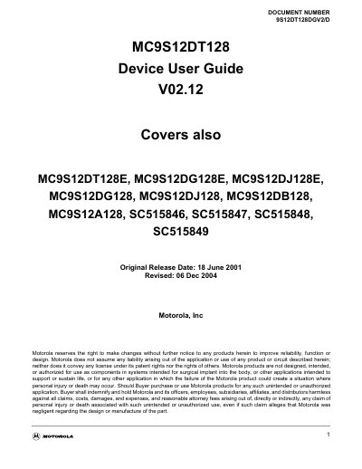
This user guide covers the MC9S12DT128 microcontroller, describing its architecture, pin functions, memory map, and peripheral blocks. It includes revision history, derivative differences, and detailed electrical characteristics.
The document also provides mechanical dimensions for the 80‑pin QFP package, power‑supply pin definitions, clock configuration, and low‑power modes, serving engineers who design and debug systems based on this device.
| Maximum VDD | 2.35 V |
|---|---|
| Minimum bus frequency | 0.25 MHz |
| Package type | 80‑pin QFP (lead‑free option available) |
The VDD voltage was increased to 2.35 V.
The minimum bus frequency is 0.25 MHz.
It is offered in an 80‑pin QFP package and a lead‑free (PVE) package option.