
STD70N02L STD70N02L-1 N-channel 24V - 0.0068 Ω - 60A - DPAK - IPAK STripFET ™ III Power MOSFET General features RDS(ON) * Qg industry’s benchmark Conduction losses reduced Switching losses reduced Low threshold device Description This series of products utilizes the latest advanced design rules of ST’s proprietary STripFET ™ technology. This is suitable for the most demanding DC-DC converter application where high efficiency is to be achieved. Applications Switching application Internal schematic diagram Type VDSS RDS(on) ID STD70N02L 24V <0.008 Ω 60A STD70N02L-1 24V <0.008 Ω 60A 1 3 3 2 1 DPAK IPAK www.st.com Order codes Part number Marking Package Packaging STD70N02L-1 D70N02L IPAK Tube STD70N02L D70N02L DPAK Tape & reel Contents STD70N02L - STD70N02L-1 2/17 Contents 1 Electrical ratings 2 Electrical characteristics 2.1 Electrical characteristics (curves) 3 Test circuits 4 Package mechanical data 5 Package mechanical data 6 Revision history
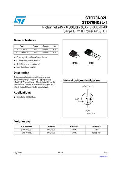
The STD70N02L is a 24 V N‑channel MOSFET with a low on‑resistance and high current capability, designed for high‑efficiency DC‑DC converter applications. It is offered in DPAK and IPAK (tube) packages and incorporates ST’s proprietary STriPFET™ technology.
The document provides absolute maximum ratings, electrical characteristics, switching times, and package mechanical data, along with revision history and legal notices. It is intended for designers and engineers selecting MOSFETs for power conversion circuits.
| Drain‑source voltage (VDS) | 30 V |
|---|---|
| Continuous drain current (Id) @ 25 °C | 60 A |
| Pulsed drain current (Id) | 240 A |
| Typical on‑resistance (RDS(on)) | 0.008 Ω |
| Input capacitance (Ciss) | 1400 pF |
| Output capacitance (Coss) | 400 pF |
| Total gate charge (Qg) | 24 nC |
| Package type | DPAK, IPAK (tube) |
The device can handle up to 60 A continuous drain current at a junction temperature of 25 °C.
The typical on‑resistance is 0.008 Ω under a test condition of VGS = 10 V and ID = 30 A.
The STD70N02L is offered in DPAK and IPAK (tube) packages.
The gate‑source threshold voltage is specified around 1 V (typical) with a test condition of VGS = Ves and ID = 250 µA.