
This document describes the features and characteristics of STMicroelectronics' STripFET™ II Power MOSFET series. This series of products, realized with the STripFET process, has exceptional dv/dt capability, low input capacitance, and gate charge. It is suitable for advanced high-efficiency isolated DC-DC converters, telecom and computer applications, and other applications with low gate charge drive requirements.
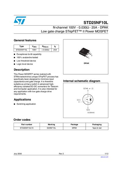
The STD25NF10L Power MOSFET series, realized with STMicroelectronics' STripFET™ II process, is designed to minimize input capacitance and gate charge, making it ideal as a primary switch in advanced high‑efficiency isolated DC‑DC converters for telecom and computer applications. It is a low‑threshold, logic‑level device with exceptional dv/dt capability and 100 % avalanche testing.
Key electrical ratings include a 100 V drain‑source voltage, 25 A continuous drain current at 25 °C, 0.030–0.035 Ω on‑resistance, and a total gate charge of about 52 nC. The device is supplied in a DPAK package with a thermal resistance of 1.5 °C/W and a maximum power dissipation of 100 W at 25 °C.
| Drain‑source voltage (VDS) | 100 V |
|---|---|
| Continuous drain current (ID) at 25 °C | 25 A |
| Continuous drain current (ID) at 100 °C | 21 A |
| Thermal resistance (junction‑case) | 1.5 °C/W |
| Maximum power dissipation | 100 W |
The device can handle up to 25 A continuous drain current at 25 °C.
The part can dissipate up to 100 W at a junction temperature of 25 °C.