
This datasheet records the model, package, voltage, current, RDSon, switching time, gate voltage and other information of FGH30N6S2 / FGP30N6S2 / FGB30N6S2. This datasheet is mainly used for power factor correction (PFC) circuits, full bridge topologies, half bridge topologies, push-pull circuits, uninterruptible power supplies, zero voltage and zero current switching circuits.
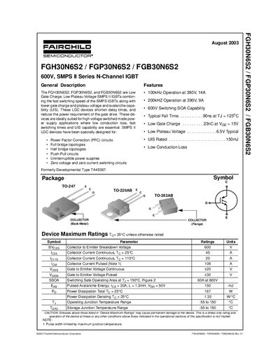
The FGH30N6S2, FGP30N6S2, and FGB30N6S2 are low‑gate‑charge, low‑plateau‑voltage SMPS II IGBTs designed for high‑voltage switched‑mode power‑supply applications. They combine fast switching with reduced gate‑drive power and include avalanche capability (UIS). Typical applications include power‑factor‑correction circuits, full‑bridge and half‑bridge topologies, push‑pull converters, uninterruptible power supplies, and zero‑voltage/zero‑current switching circuits.
Key specifications include a 600 V collector‑to‑emitter breakdown voltage, up to 45 A continuous collector current at 25 °C, low gate charge of 23 nC at VEE = 15 V, and a typical plateau voltage of 6.5 V. The devices support operation up to 200 kHz (390 V, 9 A) and dissipate up to 167 W at 25 °C. Handling precautions stress static‑discharge protection, shorted leads before assembly, grounding of the operator, and avoiding power‑on insertion.
| Collector‑to‑Emitter Breakdown Voltage (BVce) | 600 V |
|---|---|
| Continuous Collector Current (Ic) at 25 °C | 45 A |
| Gate Charge (Qg) | 23 nC at VEE = 15 V |
| Plateau Voltage (VGE) | 6.5 V typical |
| Maximum Switching Frequency | 200 kHz at 390 V, 9 A |
| Power Dissipation (Pp) at 25 °C | 167 W |
| Thermal Resistance Junction‑Case (RθJC) | 0.75 °C/W |
They are intended for power‑factor‑correction circuits, full‑bridge and half‑bridge topologies, push‑pull converters, uninterruptible power supplies, and zero‑voltage/zero‑current switching circuits.
The typical gate charge is 23 nC when the gate‑emitter voltage is 15 V.
The devices are rated for a collector‑to‑emitter breakdown voltage of 600 V.