
BSO200N03S OptiMOS®2 power transistor is a fast switching MOSFET designed for switch mode power supplies (SMPS). It features optimized technology for notebook DC/DC conversion. It is an N-channel MOSFET with logic level drive. It has excellent gate charge multiplied by on-resistance (FOM), very low on-resistance, avalanche and dv/dt ratings. It is lead-free plated and RoHS compliant.
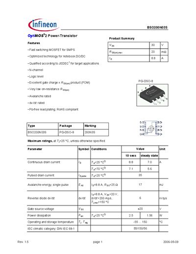
The BSO200N03S is an N‑channel, logic‑level OptiMOS®2 power MOSFET designed for SMPS and notebook DC/DC applications. It offers low on‑resistance, fast switching, and avalanche and dv/dt ratings.
Key specifications include a continuous drain current of 8.8 A at 25 °C, Rds(on) of 16.6 mΩ at Vgs = 10 V, gate threshold voltage between 1.2 V and 1.6 V, and a maximum power dissipation of 1.56 W. The device is supplied in a PG‑DSO‑8 package and operates from –55 °C to 150 °C.
| On‑state resistance (Rds(on)) | 16.6 mΩ (Vgs = 10 V) |
|---|---|
| Package | PG‑DSO‑8 |
It is supplied in a PG‑DSO‑8 surface‑mount package.