
BSS123 is a N-channel enhancement mode logic level dv/dt rated small-signal transistor.
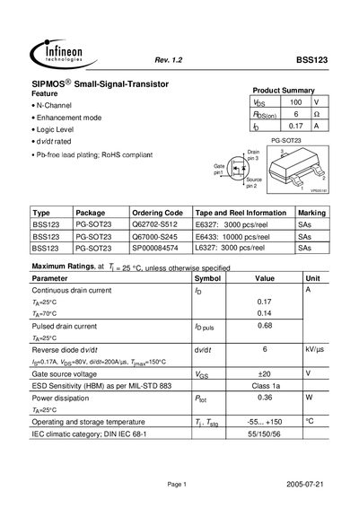
The BSS123 is an N‑channel enhancement‑mode MOSFET offered in a PG‑SOT23 package. The datasheet lists its key features, package ordering codes, and compliance information such as RoHS and Pb‑free lead plating.
Detailed sections cover thermal characteristics, static and dynamic electrical parameters, typical output and transfer curves, gate charge data, and reverse‑diode behavior, along with safe operating area and power‑dissipation limits.
| Continuous drain current (I_D) at 25 °C | 0.17 A |
|---|---|
| Pulsed drain current (I_D) at 25 °C | 0.68 A |
| Drain‑source breakdown voltage (V_DSS) | 100 V |
| Power dissipation (P_D) at 25 °C | 0.36 W |
The BSS123 can conduct a continuous drain current of 0.17 A at 25 °C.
The device is rated for a drain‑source breakdown voltage of 100 V.