
SPB17N80C3 CoolMOS® power transistor features new revolutionary high voltage technology, extreme dv/dt rating, high peak current capability, qualified according to JEDEC1) for target applications, Pb-free lead plating; RoHS compliant, ultra low gate charge and ultra low effective capacitances. CoolMOS C3 designed for: Industrial application with high DC bulk voltage; Switching Application (Active Clamp Forward Topology)
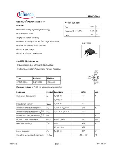
The SPB17N80C3 CoolMOS® power transistor is designed for high‑voltage industrial and switching applications. It features ultra‑low gate charge, low effective capacitances, and a rugged dv/dt rating, making it suitable for active‑clamp forward topologies and other demanding circuits.
The device is supplied in a PG‑TO263 (D2PAK) package, is RoHS‑compliant, and includes detailed electrical, thermal, and dynamic characteristics such as a continuous drain current of 17 A, a drain‑source breakdown voltage of 800 V, and a typical on‑state resistance of 0.25 Ω.
| Continuous drain current (Id) | 17 A |
|---|---|
| Pulsed drain current (Id,pulse) | 51 A |
| Drain‑source breakdown voltage (Vds) | 800 V |
| Gate threshold voltage (Vgs(th)) | 2.0 V – 3.9 V |
| On‑state resistance (Rds(on)) | 0.25 Ω typical |
| Input capacitance (Ciss) | 2300 pF |
| Output capacitance (Coss) | 100 pF max |
| Total gate charge (Qg) | 177 nC |
| Avalanche energy (single pulse) | 670 mJ |
The device can conduct a continuous drain current of 17 A at 25 °C.
The SPB17N80C3 is rated for a drain‑source breakdown voltage of 800 V.
It is supplied in a PG‑TO263 (D2PAK) surface‑mount package.
The gate threshold voltage ranges from about 2.0 V to 3.9 V.