
Infineon SPW12N50C3 Power Transistor Datasheet

This document is an TDP calculation table from Infineon, which mainly introduces how to calculate TDP
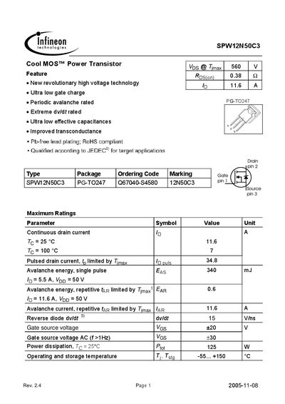

Infineon SPW12N50C3 Power Transistor Datasheet - cover page
Brand
Infineon
Category
Other Electronics
Document type
Datasheet
Language
English
Pages
11
File format
PDF
File size
932 KB
Published
06 April, 2012
Updated
30 September, 2023
MD5 checksum
4670EC358CFB1C07C6FAE0118E0755C6

About this manual

The SPW12N50C3 is a 560 V, 11.6 A Cool MOS™ power transistor featuring ultra‑low gate charge, low on‑resistance, and high avalanche capability. The datasheet provides detailed electrical, thermal, and safe‑operating‑area characteristics for designers.

Key sections include maximum ratings, thermal characteristics, electrical parameters, transient thermal impedance, and typical output characteristics, allowing engineers to evaluate performance and integrate the device into high‑voltage applications.

What's inside

  • Maximum Ratings
  • Thermal Characteristics
  • Electrical Characteristics
  • Transient Thermal Impedance
  • Safe Operating Area
  • Typical Output Characteristics
  • Drain‑source On‑Resistance
  • Gate Charge Characteristics
  • Avalanche Energy

Specifications

Drain‑source voltage (VDS)560 V

Frequently asked questions

What is the rated drain‑source voltage for this transistor?

The SPW12N50C3 is rated for a maximum drain‑source voltage of 560 V.

Download PDF (932 KB)

More Infineon Manuals


View all Infineon manuals →