
BTS 7710 GP is part of the TrilithIC family, containing three dies in one package: one double high-side switch and two low-side switches. It is optimized for DC motor management applications and features low RDS ON, maximum peak current, and very low quiescent current.
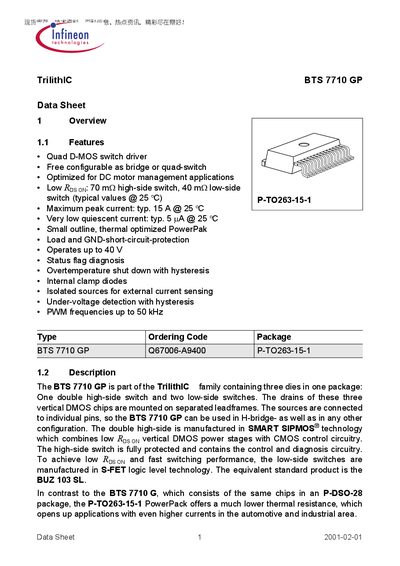
The BTS 7710 GP is a quad D‑MOS switch driver offered in a P‑TO263‑15‑1 PowerPak package. It can be configured as a bridge or as four independent switches and is optimized for DC motor management, featuring low on‑resistance, high peak current capability, and integrated protection functions.
The datasheet includes pin configurations, functional block diagrams, circuit description, electrical characteristics, absolute maximum ratings, operating ranges, and package dimensions, giving designers the information needed to integrate the device into automotive and industrial applications.
| Maximum peak current (typical) | 15 A @ 25 °C |
|---|---|
| Quiescent current (typical) | 5 pA @ 25 °C |
| Operating voltage range | 3 V – 42 V |
| Maximum supply voltage | 40 V |
| PWM frequency range | up to 50 kHz |
| Drain‑source breakdown voltage | 55 V |
| Thermal resistance (junction‑case, HS path) | 1.7 K/W |
The device can handle a typical peak current of 15 A at 25 °C.