
This data sheet introduces the BTS 7700 G features including low RDS ON, maximum peak current, very low quiescent current, load and GND short-circuit protection, operating voltage, status flag diagnosis, overtemperature shut down, internal clamp diodes, isolated sources for external current sensing, under-voltage detection and PWM frequencies
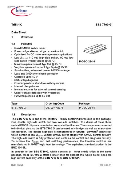
The BTS 7700 G is a quad D‑MOS switch driver from Infineon’s TrilithIC family. It integrates one double high‑side switch and two low‑side switches in a single package, offering configurable bridge or quad‑switch operation, low on‑resistance, and protection features such as short‑circuit and over‑temperature shutdown.
The datasheet details the pin configuration, functional block diagram, circuit description, absolute maximum ratings, operating range, and package dimensions. It also lists electrical characteristics like peak current, quiescent current, PWM frequency limits, and supply voltage requirements, helping designers select and implement the device in DC motor management applications.
| Maximum peak current | typ. 9 A @ 25 °C |
|---|---|
| Quiescent current | typ. 5 pA @ 25 °C |
| Operating voltage | up to 40 V |
| PWM frequency | up to 50 kHz |
| Supply voltage range | 3 V – 42 V |
| Integrated dies | Three dies in one package |
The device can handle a typical peak current of 9 A at 25 °C.
It operates up to 40 V, with a supply voltage range from 3 V to 42 V.
The IC contains one double high‑side switch and two low‑side switches, totaling three switches in one package.
It provides load and ground short‑circuit protection, over‑temperature shutdown with hysteresis, undervoltage lockout, and internal clamp diodes.