
SPP11N65C3, SPA11N65C3 SPI11N65C3 Cool MOS™ Power Transistor features 650 V VDS, 0.38 RDS(on) and 11 A ID. Its features are new revolutionary high voltage technology, ultra low gate charge, periodic avalanche rated, extreme dv/dt rated, high peak current capability and improved transconductance.
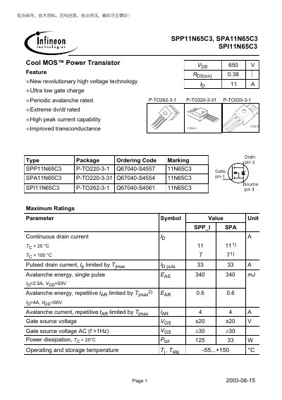
The Cool MOS™ Power Transistor family from Infineon offers high‑voltage capability (VDS up to 650 V) with low on‑state resistance and high peak current capability. Three package variants are covered: P‑TO‑220‑3‑1, P‑TO‑220‑3‑31 and P‑TO‑262‑3‑1, each identified by distinct marking codes.
The datasheet lists maximum ratings, thermal characteristics, detailed electrical parameters, transient thermal impedance, safe operating area curves and mechanical dimensions. It also includes packaging information, ordering codes and regulatory notices.
| Maximum Drain‑Source Voltage (VDS) | 650 V |
|---|---|
| On‑State Resistance (RDS(on)) | 0.38 Ω (typical) |
| Junction‑to‑Case Thermal Resistance (RthJC) | 1 K/W |
The device is rated for a maximum drain‑source voltage of 650 V.
The typical on‑state resistance is 0.38 Ω.