
The MAX5058/MAX5059 enable secondary-side synchronous rectification in isolated power supplies using widely available power MOSFETs. These devices facilitate the commutation of the secondary-side MOSFETs by providing a clean gate-drive signal that is synchronized to the power MOSFET switching in the primary side of the isolation transformer. The MAX5058/MAX5059 complement the MAX5051 and MAX5042/MAX5043 primary-side PWM ICs and enable the design of high-efficiency synchronously rectified isolated power supplies. Simultaneous conduction of the primary side and the freewheeling synchronous rectifier MOSFET is avoided by having a look-ahead signal (before the primary-side MOSFETs turn ON), thus eliminating large current spikes resulting from a shorted transformer secondary. An on-board error amplifier with a versatile current reference output enables virtually unlimited possibilities in reference-voltage generation. Reference voltage for the error amplifier is generated by connecting an appropriate resistor to this output. Low on-resistance margining MOSFETs integrated on-chip allow for implementation of a margining circuit without the use of external switches. The MAX5058 provides a 5V LDO output for logic-level MOSFETs while the MAX5059 provides a 10V LDO output for conventional 10V MOSFETs. The MAX5058/MAX5059 are designed to enable paral- leling of multiple power supplies for accurate current sharing using a sim
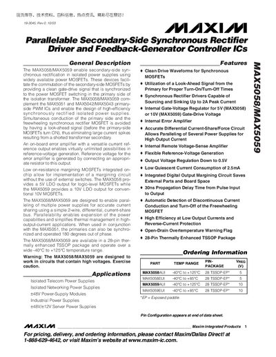
The MAX5058 and MAX5059 are parallelable secondary‑side synchronous rectifier driver and feedback‑generator controller ICs. They enable high‑efficiency isolated power supplies by providing clean gate‑drive waveforms synchronized to the primary‑side MOSFET switching and include on‑chip error amplifiers, LDO regulators (5 V for MAX5058, 10 V for MAX5059), and a differential current‑share bus for paralleling multiple supplies.
The devices are offered in a 28‑pin thermally‑enhanced TSSOP package and operate from –40 °C to +125 °C. Typical applications include isolated telecom and networking power supplies, +48 V server modules, and industrial power supplies. Detailed electrical characteristics, absolute maximum ratings, and typical operating curves are provided in the document.
| Peak Source / Sink Current | 2 A |
|---|---|
| Propagation Delay | 30 ns |
| Operating Temperature Range | -40 °C to +125 °C |
| Package | 28‑Pin Thermally Enhanced TSSOP |
The MAX5058 provides a 5 V LDO output for logic‑level MOSFETs.
The driver can source and sink up to 2 A peak current.
Both devices operate from –40 °C to +125 °C.
They are supplied in a 28‑pin thermally enhanced TSSOP package.