
The TC7WB383FK is a low on-resistance, high-speed CMOS 2-bit bus exchange switch. This bus switch allows the connections or disconnections to be made with minimal propagation delay while maintaining low power dissipation which is the feature of CMOS. When output enable (OE) is at high level, the switches are off. When at low level, the switches are on, and by the logic of EX terminal, it can choose whether 2 bits data are transferred to the corresponding terminal as it is, or the data are transferred to a terminal with exchanging data line. Therefore, it may be used as 2 to 1 multiplexer switch. Since the switch channels consist of N type MOSFET, the high level output voltage is provided about 1 V lower than VCC level. All inputs are equipped with protection circuits to protect the device from static discharge.
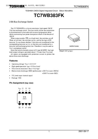
The TC7WB383FK is a low‑on‑resistance, high‑speed CMOS 2‑bit bus exchange switch. It provides selectable data routing with minimal propagation delay and low power dissipation. The device includes protection circuits for static discharge and operates from a 4.5 V to 5.5 V supply.
The datasheet lists electrical characteristics, maximum ratings, recommended operating conditions, package dimensions (US8/SSOP8‑P‑0.50A) and usage restrictions for safety‑critical applications.
| Operating voltage (Voc) | 4.5 ~ 5.5 V |
|---|---|
| Propagation delay (tpd) | 0.25 ns (max) |
| ESD performance | +200 V (JEITA), +2000 V (MIL) |
| Package type | US8 (SSOP8‑P‑0.50A) |
| Weight | 0.01 g (typ.) |
| Power dissipation (Pp) | 200 mW |
| Switch I/O current (Is) | 128 mA |
The device operates from 4.5 V to 5.5 V.
It is supplied in a US8 (SSOP8‑P‑0.50A) package.
The propagation delay is up to 0.25 ns.