
This document describes the features of TC7SH08FS, a TOSHIBA CMOS digital integrated circuit, including high speed, low power dissipation, high noise immunity, and wide operating voltage range.
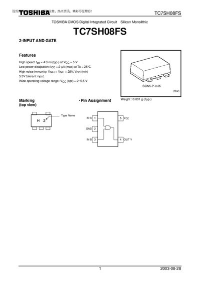
The TC7SHO8FS is a 2‑input AND gate CMOS digital integrated circuit offering high speed (tpd = 4.3 ns typ. at Vcc = 5 V) and ultra‑low power dissipation (Icc = 2 pA max at 25 °C). It operates over a wide voltage range (Vcc = 2 ~ 5.5 V) and includes 5‑V tolerant inputs.
The document lists maximum ratings, detailed DC and AC electrical characteristics, package dimensions (SON5‑P‑0.35) and weight (0.001 g typ.), and outlines usage restrictions, emphasizing that the device is not intended for safety‑critical or high‑reliability applications such as medical or aerospace equipment.
| Propagation delay (tpd) | 4.3 ns typ. at Vcc = 5 V |
|---|---|
| Supply current (Icc) | 2 pA max at 25 °C |
| Operating voltage range (Vcc) | 2.0 ~ 5.5 V |
| Supply voltage range | -0.5 ~ 7.0 V |
| Power dissipation (Pp) | 50 mW |
| Package type | SON5‑P‑0.35 |
| Weight | 0.001 g typ. |
The typical propagation delay is 4.3 ns at a supply voltage of 5 V.
The device can be powered from –0.5 V to 7.0 V, with a recommended operating range of 2.0 V to 5.5 V.
The maximum power dissipation is rated at 50 mW.
Yes, it is not intended for safety‑critical or high‑reliability applications such as medical, aerospace, or traffic‑signal equipment.