
This document introduces the technical specifications of TMS320F2810 and TMS320F2812 digital signal processors, including high-performance static CMOS technology, 150 MHz (6.67-ns cycle time), low-power (1.8-V core, 3.3-V I/O) design, 3.3-V flash programming voltage, high-performance CPU (C28x), 16 x 16 and 32 x 32 MAC operations, 16 x 16 dual MAC, Harvard bus architecture, atomic operations, fast interrupt response and processing, unified memory programming model, 4M linear program address reach, 4G linear data address reach, code-efficient (in C/C++ and Assembly), and TMS320F24x/LF240x processor source code compatible.
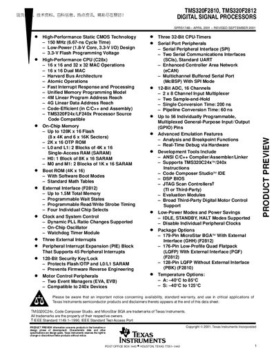
The TMS320F2810 and TMS320F2812 are 150 MHz (6.67 ns cycle) C28x digital signal processors built on a high‑performance static CMOS technology. They feature a Harvard bus architecture, up to 128 KB of on‑chip flash, 18 KB of single‑access RAM, a 12‑bit 16‑channel ADC, and extensive motor‑control peripherals such as two event managers (EVA, EVB) and up to 56 programmable GPIO pins.
The devices are offered in three package options—179‑pin MicroStar BGA, 176‑pin low‑profile QFP, and 128‑pin QFP—covering temperature ranges from –40 °C to 85 °C (extended to –40 °C to 125 °C). The datasheet includes functional block diagrams, pin‑function tables, memory maps, and detailed electrical and mechanical specifications.
| Maximum CPU Frequency | 150 MHz (6.67 ns cycle) |
|---|---|
| Core Voltage | 1.8 V |
| On‑Chip Flash (F2810) | 64 KB |
| Single‑Access RAM (SARAM) | 18 KB |
| ADC Resolution | 12‑bit |
| Number of GPIO Pins | 56 |
| Operating Temperature Range | -40 °C to 85 °C (standard), -40 °C to 125 °C (extended) |
The core operates at 1.8 V.
Up to 56 individually programmable GPIO pins are provided.
Standard devices operate from –40 °C to 85 °C, with an extended range up to –40 °C to 125 °C.