
This data sheet provides complete design documentation for the second-generation devices of the TMS320 family.
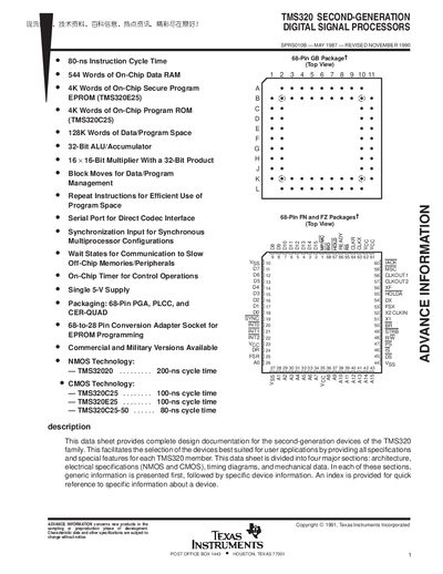
This datasheet provides complete design documentation for the second‑generation devices of the TMS320 family, including the TMS32020, TMS320C25, TMS320C25‑50, and TMS320E25. It covers architecture, electrical specifications, timing diagrams, mechanical data, and pin assignments to help engineers select the appropriate device for their applications.
The document also includes key features such as instruction cycle times, on‑chip memory sizes, 32‑bit ALU, 16×16‑bit multiplier, serial ports, and packaging options (68‑pin PGA, PLCC, CER‑QUAD). A package option addendum lists the status and environmental classifications of each part.
| Instruction Cycle Time (TMS320C25‑50) | 80 ns |
|---|---|
| Instruction Cycle Time (TMS320C25) | 100 ns |
| On‑Chip Data RAM | 544 Words |
| On‑Chip Program ROM | 4K Words |
| On‑Chip Secure Program EPROM (TMS320E25) | 4K Words |
| ALU/Accumulator Width | 32‑bit |
| Supply Voltage | Single 5‑V Supply |
| Package Types | 68‑Pin PGA, PLCC, CER‑QUAD |
The TMS320C25 has an instruction cycle time of 100 ns.
The TMS32020 provides 544 words of on‑chip data RAM.
They are offered in 68‑Pin PGA, PLCC, and CER‑QUAD packages.
The TMS320E25 uses a 4K‑word on‑chip secure program EPROM.