
This document describes the features and characteristics of DSP controllers including TMS320LF2407A, TMS320LF2406A, TMS320LF2403A, TMS320LF2402A, TMS320LC2406A, TMS320LC2404A, TMS320LC2403A, TMS320LC2402A. These products are based on the TMS320C2xx DSP CPU core and feature high-performance static CMOS technology, 25-ns instruction cycle time (40 MHz), 40 MIPS performance, and low-power 3.3V design. They offer options for Flash (LF) and ROM (LC) devices, and include various on-chip memory such as Flash EEPROM or ROM, data/program RAM, and dual-access RAM. Additionally, they support SCI/SPI bootloader and multiple event-manager (EV) modules, which include 16-bit general-purpose timers, 16-bit pulse-width modulation (PWM) channels, input qualifier, etc.
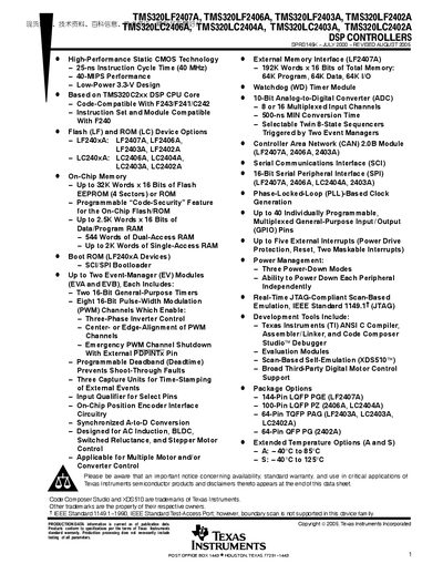
The TMS320LF2407A is a member of the TMS320C24x™ generation of fixed‑point digital signal processors. It offers a 25‑ns instruction cycle, 40 MIPS performance at 40 MHz, and a rich set of peripherals optimized for motor‑control and power‑conversion applications.
Key features include up to 32 K words of on‑chip flash, 544 words of dual‑access RAM, a 10‑bit ADC with 500 ns minimum conversion time, eight PWM channels, CAN 2.0B, SPI and SCI communication interfaces, and up to 40 programmable GPIO pins. The device is supplied in various LQFP and TQFP packages and supports multiple power‑down modes for low‑power operation.
| Instruction Cycle Time | 25 ns |
|---|---|
| Performance | 40 MIPS at 40 MHz |
| On‑Chip Flash Memory | Up to 32 K words × 16 bits |
| On‑Chip RAM | 544 words (dual‑access) |
| External Memory Interface | 192 K words total (64 K program, 64 K data, 64 K I/O) |
| ADC Resolution | 10‑bit |
| ADC Minimum Conversion Time | 500 ns |
| PWM Channels | Eight 16‑bit PWM channels |
| GPIO Pins | Up to 40 programmable pins |
| CAN Interface | CAN 2.0B module |
The device has a 25‑ns instruction cycle.
Up to 40 GPIO pins are individually programmable.
It includes a CAN 2.0B module, a 16‑bit SPI interface, and an SCI (asynchronous serial) interface.