
This document describes the features and characteristics of DSP controllers TMS320LF2407, TMS320LF2406, TMS320LF2402, TMS320LC2406, TMS320LC2404, and TMS320LC2402. It includes 33-ns instruction cycle time, 30 MIPS performance, low-power 3.3V design, based on T320C2xx DSP CPU core, flash and ROM device options, on-chip memory, boot ROM, and two event manager modules.
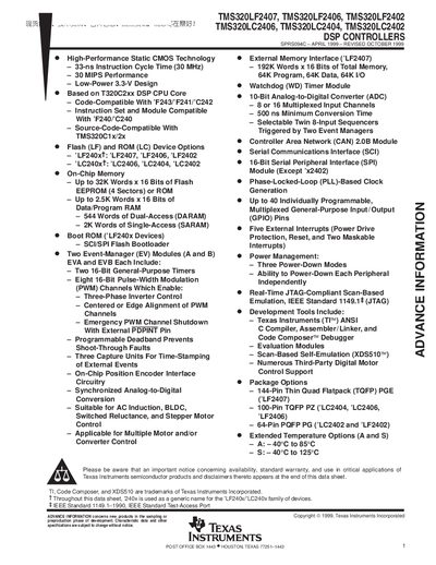
The TMS320LF240x family of digital signal processors (DSP) provides a high‑performance, low‑power solution for motor‑control and power‑conversion applications. The devices share a common C2xx core, 30 MIPS performance at 30 MHz, and a range of memory options from flash to ROM.
Key peripherals include a 10‑bit ADC with up to 16 channels, CAN 2.0B, SCI, and SPI communication modules, multiple event‑manager modules for PWM generation, and extensive GPIO resources. The family is offered in several QFP packages (144‑pin, 100‑pin, 64‑pin) with temperature ranges from –40 °C to 125 °C.
| Instruction Cycle | 33 ns |
|---|---|
| Performance | 30 MIPS |
| Supply Voltage | 3.3 V |
| Flash Memory | Up to 32K words × 16‑bit |
| DARAM | 544 words |
| SARAM | 2K words |
| ADC Resolution | 10‑bit |
| GPIO Pins | 41 shared digital I/O pins |
| General‑Purpose Timers | 4 timers |
| PWM Channels | Up to 16 channels |
| CAN Interface | Supported (2.0B) |
| Package Type | 144‑pin TQFP (others available) |
The instruction cycle time is 33 ns.
The devices provide a 10‑bit ADC with up to 16 input channels.
They operate from a 3.3 V supply.
The family includes CAN 2.0B, SCI (asynchronous serial), and SPI (16‑bit synchronous) interfaces.