
This document details the features of TMS320LF2407, TMS320LF2406, TMS320LF2402 TMS320LC2406, TMS320LC2404, TMS320LC2402 DSP CONTROLLERS, including high-performance static CMOS technology, 33-ns instruction cycle time, 30 MIPS performance, low-power 3.3-V design, based on T320C2xx DSP CPU core, code compatible ’F243/’F241/’C242, instruction set and module compatible ’F240/’C240, source code compatible TMS320C1x/2x, Flash (LF) and ROM (LC) device options, on-chip memory, boot ROM (’LF240x devices), SCI/SPI flash bootloader, two event manager (EV) modules (A and B) EVA and EVB each include two 16-bit general-purpose timers, eight 16-bit pulse-width modulation (PWM) channels, three capture units, on-chip position encoder interface circuitry, synchronous analog-to-digital conversion, suitable for AC induction, BLDC, switched reluctance and stepper motor control, application for motor control, automotive applications, digital control, instrumentation and instruments, power management, telecommunications, industrial control and other fields.
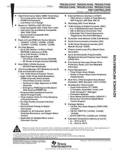
The TMS320LF240x and TMS320LC240x devices are members of Texas Instruments' 24x family of fixed‑point digital signal processors. They combine a high‑performance C2000 core with integrated peripherals for motor control, power conversion, and general‑purpose applications.
Key capabilities include a 33‑ns instruction cycle (30 MIPS at 30 MHz), up to 32 K words of flash, a 10‑bit ADC with 500 ns minimum conversion time, multiple event‑manager modules, CAN 2.0B, SPI, SCI, and extensive GPIO and PWM resources. The datasheet provides detailed pin‑out tables, memory maps, and mechanical dimensions for the 144‑pin, 100‑pin, and 64‑pin QFP packages.
| Instruction Cycle | 33 ns |
|---|---|
| Performance | 30 MIPS (30 MHz) |
| Supply Voltage | 3.3 V |
| Flash Memory | Up to 32 K words × 16 bits |
| ADC Resolution | 10‑bit |
| Minimum ADC Conversion Time | 500 ns |
| GPIO Pins | 41 digital I/O pins (shared) |
| PWM Channels | 10 PWM compare outputs |
| CAN Interface | CAN 2.0B (available on LF2407, LF2406, LF2404) |
The instruction cycle time is 33 ns.
They operate from a 3.3 V supply.
Yes, a CAN 2.0B module is included on the LF2407, LF2406, and LF2404 devices.