
ISL6622B is a high frequency MOSFET driver from ISL designed to work with VR11.1 controllers for driving upper and lower power N-channel MOSFETs in a synchronous rectified buck converter topology. When ISL6622B detects a PSI PWM protocol sent by an Intersil VR11.1 controller, it activates Diode Emulation (DE) operation; otherwise, it operates in normal Continuous Conduction Mode (CCM) PWM mode. In the 8 Ld SOIC package, the ISL6622B drives the upper gate to 12V while the lower drive voltage is fixed at 5.75V. The 10 Ld DFN part offers more flexibility: the upper gate can be driven from 5V to 12V via the UVCC pin, while the lower gate has a resistor-selectable drive voltage of 5.75V, 6.75V, and 7.75V (typical). This provides the flexibility necessary to optimize applications involving trade-offs between gate charge and conduction losses. ISL6622B employs a high-frequency, high-efficiency synchronous rectified buck converter topology to provide excellent light load efficiency.
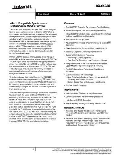
The ISL6622B MOSFET driver from Intersil provides dual upper and lower gate drives for synchronous rectified buck converters. It supports advanced PWM protocols, diode‑emulation for light‑load efficiency, and an internal LDO that allows selectable lower‑gate drive voltages.
The device is offered in 8‑lead SOIC and 10‑lead DFN packages, operates from 6.8 V to 13.2 V (VCC) with UVCC ranging 5 V‑12 V, and includes features such as adaptive shoot‑through protection, pre‑POR over‑voltage protection, and a 36 V internal bootstrap diode.
| Upper gate drive voltage (SOIC) | 12 V |
|---|---|
| Lower gate drive voltage (SOIC) | 5.75 V |
| Upper gate drive voltage (DFN) | 5 V‑12 V (via UVCC pin) |
| Lower gate drive voltage (DFN) | 5.75 V, 6.75 V, 7.75 V (selectable) |
| Supply voltage (VCC) range | 6.8 V‑13.2 V |
| Maximum junction temperature | +150 °C |
| Sinking current capability (lower gate) | 3 A |
It turns off the lower MOSFET when the inductor current reaches zero, allowing discontinuous conduction mode and improving light‑load efficiency.
VCC operates from 6.8 V to 13.2 V, while UVCC can be supplied between 5 V and 12 V.